Substrate for optical semiconductor apparatus, method for manufacturing the same, optical semiconductor apparatus and method for manufacturing the same

a technology of optical semiconductor and substrate, which is applied in the direction of optical articles, coatings, other domestic articles, etc., can solve the problems of uneconomic method, inability to electrically connect between optical semiconductor devices, and inability to manufacture stably optical semiconductor apparatuses with high luminance, etc., and achieves high reflection efficiency, high quality, and easy manufacturing

Inactive Publication Date: 2013-11-14
SHIN ETSU CHEM IND CO LTD
View PDF8 Cites 5 Cited by
  • Summary
  • Abstract
  • Description
  • Claims
  • Application Information

AI Technical Summary

Benefits of technology

[0048]By such a manufacturing method, an optical semiconductor apparatus having higher reflection efficiency and high quality in which the generation of a flash burr is inhibited can be readily manufactured with a low cost.

Problems solved by technology

In manufacture of the substrate, however, transfer molding, which produces a large amount of cured resin unnecessary for products called “cull” is formed in a resin passage of the mold during molding as well known, is used, so that the method is uneconomical.
The resin burr contaminates the surface of the leads to be utilized for wire bonding connection of the optical semiconductor device, causing failure such as inability to electrically connect between the optical semiconductor device with the leads.
Moreover, the flash burr lowers glossiness of the surface of the lead frame or the metal plating, and reflection efficiency of light emitted from the optical semiconductor apparatus, so that it causes a problem that an optical semiconductor apparatus having high luminance cannot be manufactured stably.
However, all the methods damage the surface of metal such as metal plating represented by, in particular, glossy silver plating, so that the glossiness before removing the burr cannot be maintained.
Also, a heat treatment method represented by a laser process, generates heat and the heat causes oxidation or burning on the metal surface; similarly the glossiness before removing the burr cannot be maintained.

Method used


Image

  • Substrate for optical semiconductor apparatus, method for manufacturing the same, optical semiconductor apparatus and method for manufacturing the same
  • Substrate for optical semiconductor apparatus, method for manufacturing the same, optical semiconductor apparatus and method for manufacturing the same
  • Substrate for optical semiconductor apparatus, method for manufacturing the same, optical semiconductor apparatus and method for manufacturing the same

Examples


example 1

[0118]

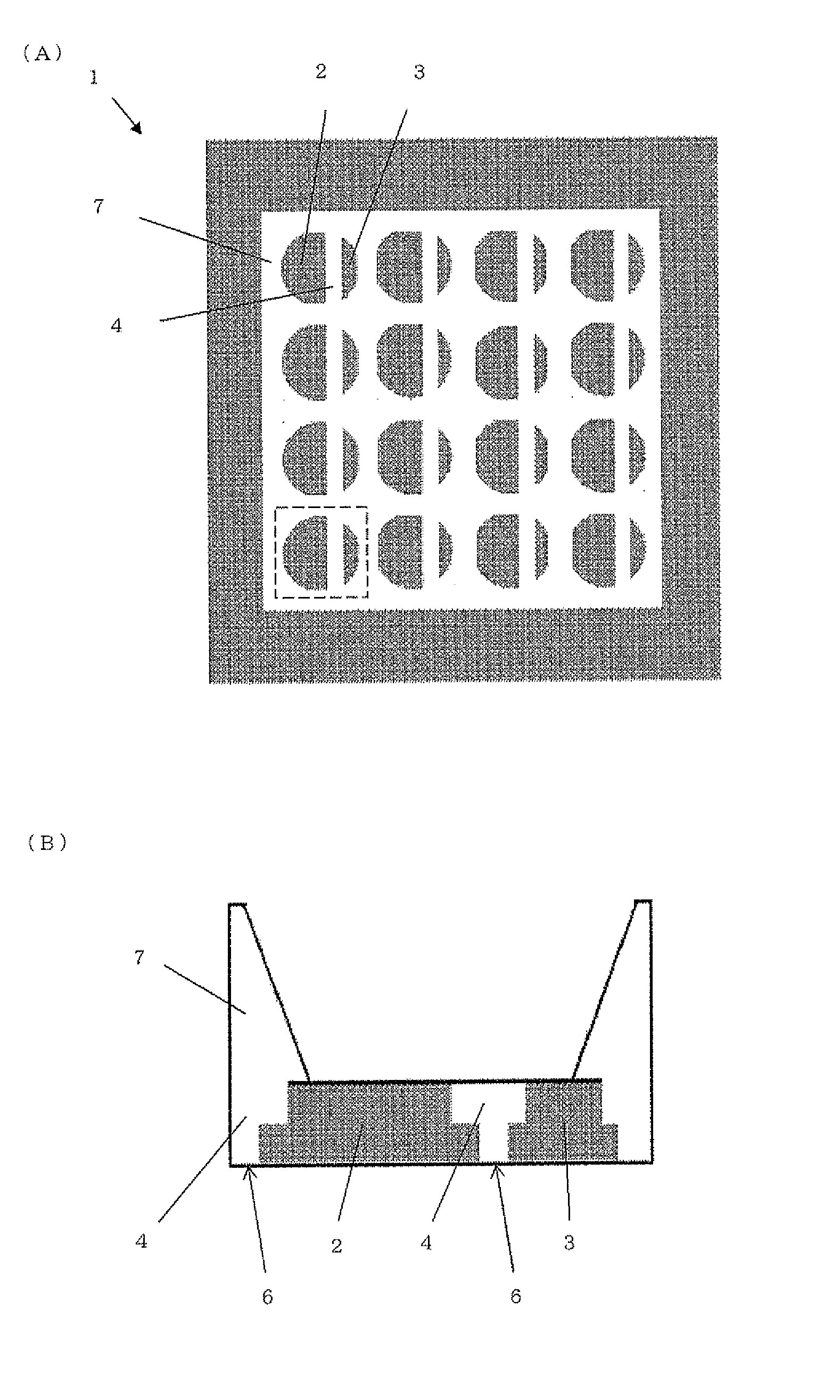
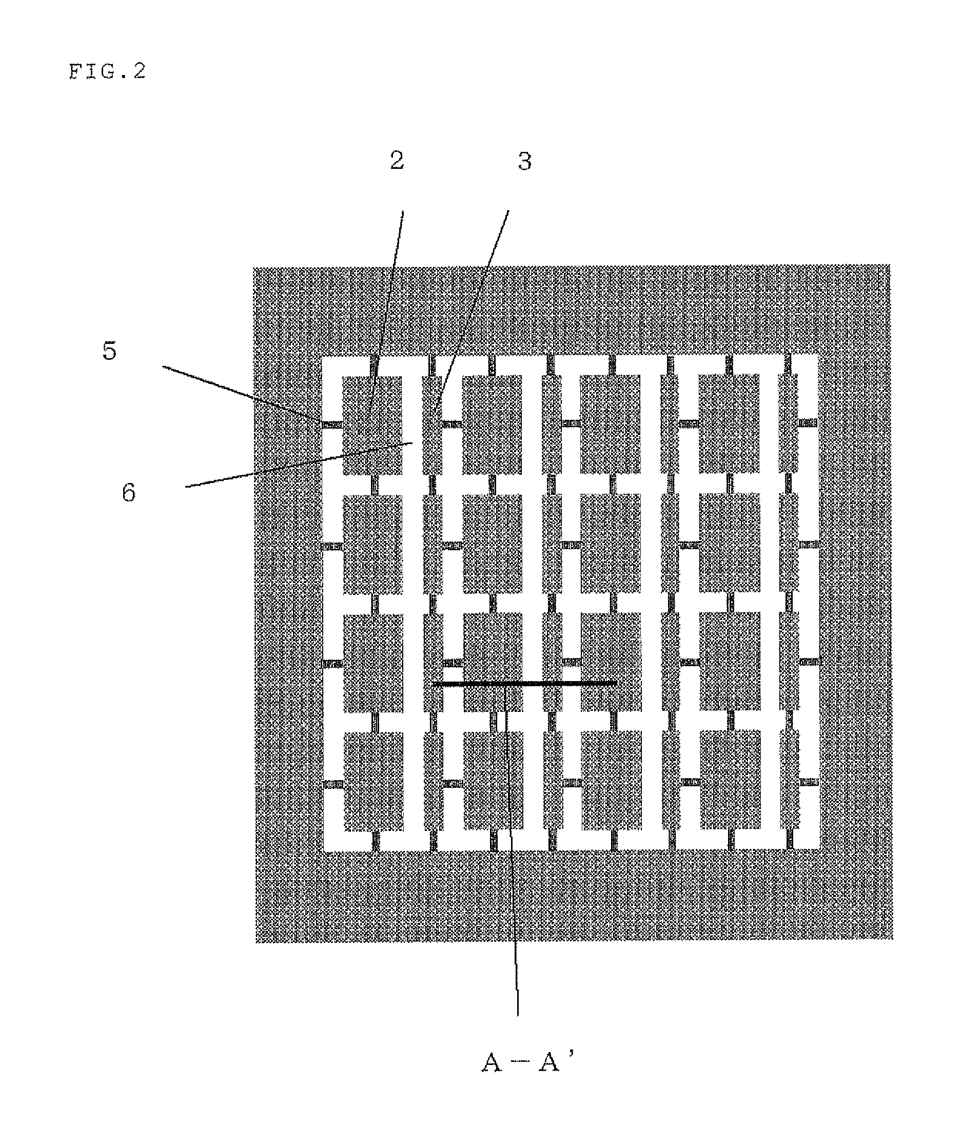
[0119]A metal plate of a copper alloy containing chromium-tin-zinc with a thickness of 0.3 mm was punched to prepare a lead frame, having a shape shown in FIG. 2, in which first leads and second leads were arranged each in parallel and connected through a tie bar. Also, an etching process was performed to form steps having a height in the thickness direction of 150 μm (½t) at the side surfaces of the first leads and the second leads, as shown at (B) in FIG. 3. Silver plating was then applied to the lead frame as metal plating. The glossiness of the metal plating was measured by using Micro Spectrophotometer VSS400A manufactured by NIPPON DENSHOKU INDUSTRIES Co., LTD. The measured points were five points, and its average value was obtained. As a result, the glossiness was 1.40.

[0120]The lead frame was fixed to the lower mold heated to 130° C. The lead frame was interposed with the upper mold heated similarly to 130° C. for mold clamping.

[0121]Next, the resin molded body and the...

example 2

[0129]A substrate for an optical semiconductor apparatus was manufactured in the same conditions as in Example 1 except that degrease cleaning was not performed, and by using the substrate for an optical semiconductor apparatus, an optical semiconductor apparatus was manufactured in the same conditions as in Example 1.

[0130]The manufactured substrate for an optical semiconductor apparatus as above was molded without an unfilled portion of the thermosetting resin, air remaining, and a flash burr. Also, when the glossiness of the metal plating was measured, it was 1.38; it was confirmed that reduction in the glossiness was inhibited as compared with the results of the later-described Comparative Examples 1 to 3.

[0131]Also, the obtained optical semiconductor apparatus was thin and had high product-dimensional accuracy.


PUM


Abstract

The present invention provides a substrate for an optical semiconductor apparatus for mounting optical semiconductor devices, the substrate includes first leads to be electrically connected to first electrodes of the optical semiconductor devices and second leads to be electrically connected to second electrodes of the optical semiconductor devices, wherein the first leads and the second leads are arranged each in parallel, a molded body of a thermosetting resin composition is molded in a penetrating gap between the first leads and the second leads, a reflector of the thermosetting resin composition is molded at a periphery of respective regions on which the optical semiconductor devices are to be mounted, and the resin molded body and the reflector are integrally molded with the first leads and the second leads by injection molding.

Description

BACKGROUND OF THE INVENTION[0001]1. Field of the Invention[0002]The present invention relates to a substrate for an optical semiconductor apparatus suitable for mounting an optical semiconductor device such as LED and a method for manufacturing the substrate, and an optical semiconductor apparatus using the substrate, and a method for manufacturing the apparatus.[0003]2. Description of the Related Art[0004]An optical semiconductor device such as LED has excellent characteristics of less electric power consumption, so that the applications of the optical semiconductor device for exterior illumination and automobile are increasing in recent years. A surface-mount optical semiconductor apparatus has been used to downsize and thin packages for such applications.[0005]The conventional surface-mount optical semiconductor apparatus has a structure having a first lead which also serves as a pad for mounting an optical semiconductor device, a second lead and a resin molded body (reflector) w...

Claims


Application Information

Patent Timeline
Patent Type & Authority Applications(United States)
IPC IPC(8): H01L33/58H05K1/03
CPCH01L33/58H05K1/0306H01L24/97H01L33/486H01L33/60H01L2224/45144H01L2224/48091H01L2224/48247H01L2224/48257H01L2924/12042H01L2924/181H01L2924/00014H01L2924/00H01L2924/00012H01L33/48H01L33/52H01L33/62
Inventor ONAI, SATOSHIIWATA, MITSUHIROHARADA, YOSHIFUMIKIMURA, SHINJI
Owner SHIN ETSU CHEM IND CO LTD
Why Eureka
Try Eureka