Surface acoustic wave device

a surface acoustic wave and acoustic wave technology, applied in piezoelectric/electrostrictive/magnetostrictive devices, piezoelectric/electrostriction/magnetostriction machines, electrical equipment, etc., can solve the problems of poor improve the frequency-temperature characteristics and improve the quality of the surface acoustic wave devi

Active Publication Date: 2013-11-14
MURATA MFG CO LTD
View PDF0 Cites 11 Cited by
  • Summary
  • Abstract
  • Description
  • Claims
  • Application Information

AI Technical Summary

Benefits of technology

[0007]Preferred embodiments of the present invention provide a surface acoustic wave device that provides improved characteristics and is easily manufactured with selected combinations of materials.
[0009]This configuration increases the acoustic velocity of the resulting elastic waves, keeps the band width ratio of the elastic waves high, and reduces spurious waves.
[0013]This configuration further increases the band width ratio of the resulting elastic waves.
[0015]This configuration improves the frequency-temperature characteristics of the surface acoustic wave device.
[0017]This configuration further improves the frequency-temperature characteristics of the surface acoustic wave device.
[0018]Various preferred embodiments of the present invention provide a surface acoustic wave device that has excellent characteristics and can be easily manufactured.

Problems solved by technology

Selecting the material for the electrode fingers and the depth of the grooves in accordance with the requirements specified in Japanese Unexamined Patent Application Publication No. 2006-270906, however, can lead to poor characteristics of the surface acoustic wave device because the performance parameters of the device, e.g., the band width ratio, the resonance Q factor, and the spurious characteristics, vary with the combination of the material for the piezoelectric substrate and that for the electrode fingers.

Method used


Image

  • Surface acoustic wave device
  • Surface acoustic wave device
  • Surface acoustic wave device

Examples


Embodiment Construction

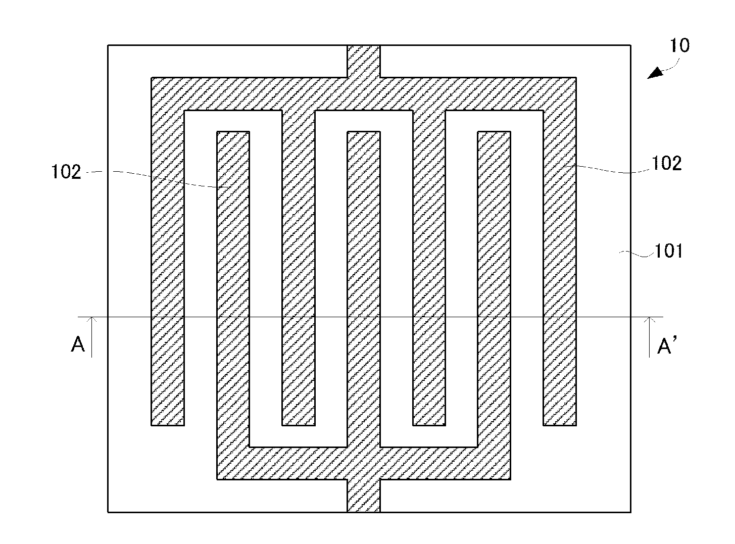
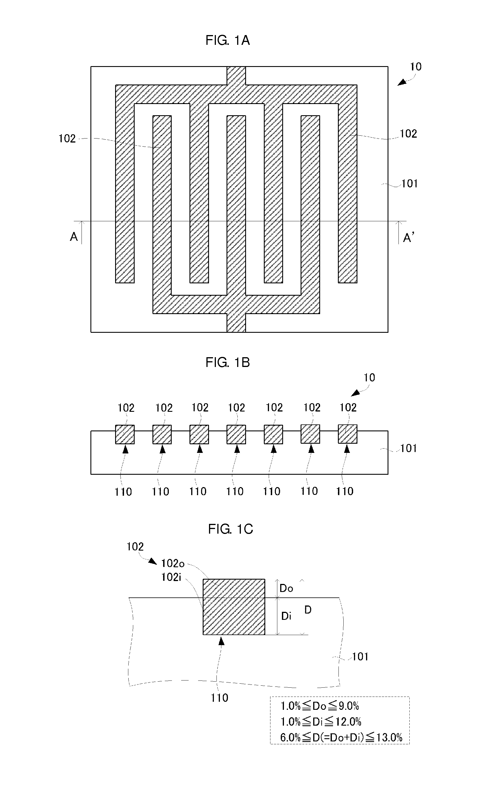
, i.e., a structure in which the entire electrodes 102 are embedded, and yet another is Comparative Example 2, i.e., a structure in which the electrodes 102 are on the surface.

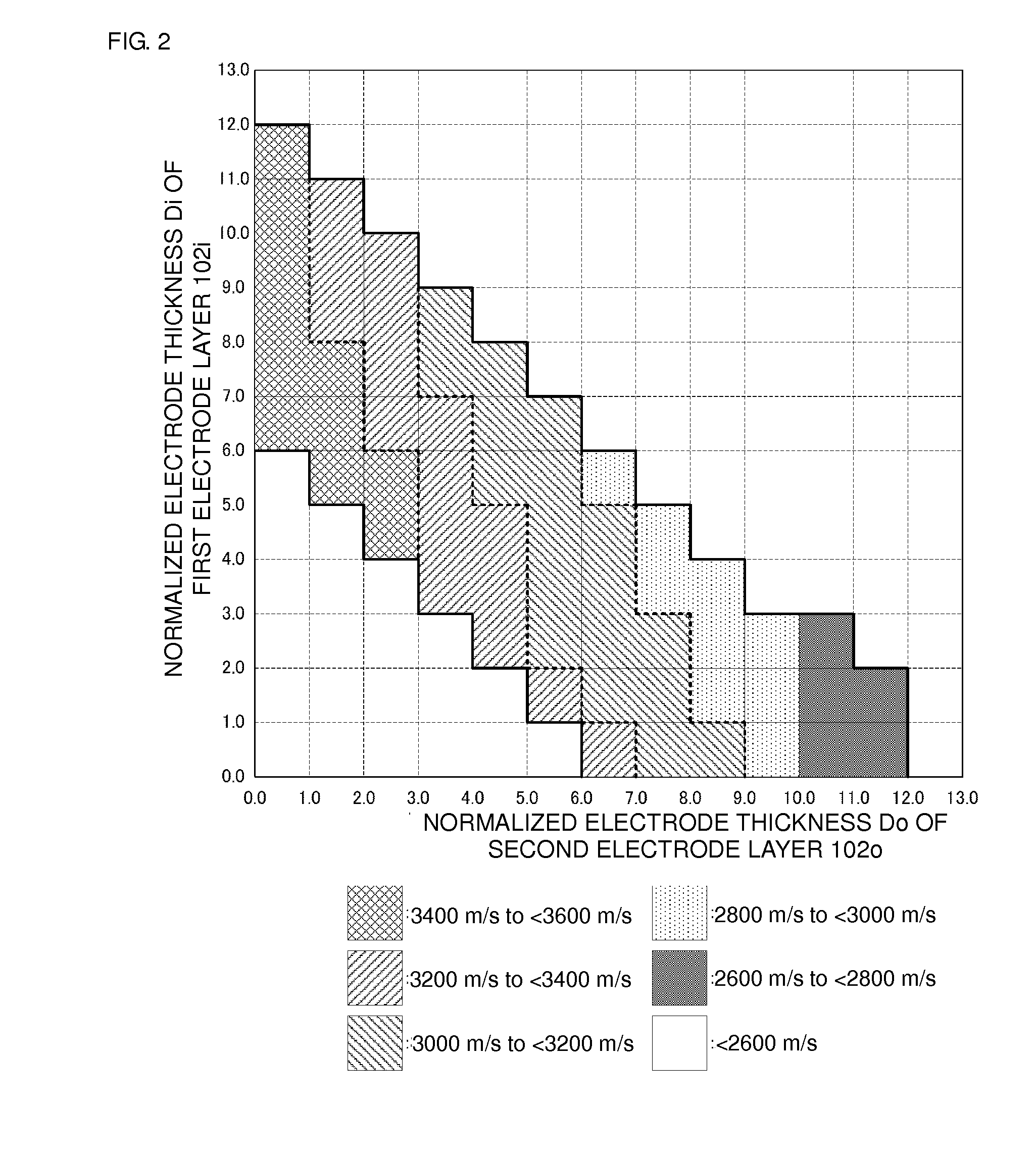
[0028]FIG. 9 shows plots of the band width ratio of Rayleigh waves against the Euler Angle θ, varying from 70° to 110°, for different proportions of the normalized electrode thickness values Do and Di of the second and first electrode layer 102o and 102i, respectively. The normalized electrode thickness D is 10%.

[0029]FIG. 10 is an enlarged partial side view of a surface acoustic wave device 10A according to another configuration of a preferred embodiment of the present invention.

[0030]FIG. 11 is a characteristic diagram showing plots of the band width ratio of SH waves as a function of the angle α made by the lateral surfaces of the grooves cut into the surface of the piezoelectric substrate and the Euler Angle θ.

[0031]FIG. 12 is an enlarged partial side view of a surface acoustic wave device 10B including an...


PUM


Abstract

A surface acoustic wave device includes a piezoelectric substrate made of lithium niobate and including grooves in a surface thereof. Each groove includes a finger of an IDT electrode made of copper. The IDT electrode includes a first electrode layer embedded in the grooves and a second electrode layer sticking out of the surface of the piezoelectric substrate. A normalized electrode thickness of the first electrode layer is about 1.0% to about 12.0% inclusive, and the normalized electrode thickness of the second electrode layer is about 1.0% to about 9.0% inclusive. The normalized electrode thickness of the entire IDT electrode is about 6.0% to about 13.0% inclusive.

Description

BACKGROUND OF THE INVENTION[0001]1. Field of the Invention[0002]The present invention relates to a surface acoustic wave device including a piezoelectric substrate and interdigital transducer (IDT) electrodes on a surface of the piezoelectric substrate.[0003]2. Description of the Related Art[0004]Hitherto researchers have created various surface acoustic wave devices that have a piezoelectric substrate and an IDT electrode on the surface of the piezoelectric substrate. For example, Japanese Unexamined Patent Application Publication No. 2006-270906 discloses a surface acoustic wave device that has a piezoelectric substrate and a plurality of electrode fingers partially embedded in the thickness direction so as to stick out or protrude from the surface.[0005]Japanese Unexamined Patent Application Publication No. 2006-270906 mentions that various known piezoelectric substrates and materials for electrode fingers can be used, and also specifies the required depth of grooves in which the...

Claims


Application Information

Patent Timeline
Patent Type & Authority Applications(United States)
IPC IPC(8): H01L41/047
CPCH01L41/047H03H9/02818H03H9/14541H10N30/87
Inventor KIMURA, TETSUYAKADOTA, MICHIO
Owner MURATA MFG CO LTD
Why Eureka
Try Eureka