Semiconductor device, and display device and electronic device having the same

a technology of semiconductor devices and electronic devices, applied in the field of semiconductor devices, can solve problems such as the breakdown of the shift register circuit, the threshold voltage rise of the transistor, and the threshold voltage of the transistor, so as to suppress the threshold voltage shift of the transistor and suppress nois

Active Publication Date: 2013-11-28
SEMICON ENERGY LAB CO LTD
View PDF1 Cites 45 Cited by
  • Summary
  • Abstract
  • Description
  • Claims
  • Application Information

AI Technical Summary

Benefits of technology

[0041]A semiconductor device of the invention can turn on a transistor, on / off of which is controlled by a signal supplied to a third wiring at regular intervals. Thus, since the transistor of a shift register circuit which uses the semiconductor device of the invention is not always on in a non-selection period, the threshold voltage shift of the transistor can be suppressed. In addition, a power supply potential is supplied to an output terminal of the shift register circuit which uses the semiconductor device of the invention through the transistor at regular intervals. Therefore, the shift register circuit which uses the semiconductor device of the invention can suppress noise which is generated in the output terminal.

Problems solved by technology

In particular, a threshold voltage shift where the threshold voltage of a transistor rises becomes obvious when the characteristics of the transistor deteriorate.
This threshold voltage shift is one of big causes of the malfunction of the shift register circuit.

Method used


Image

  • Semiconductor device, and display device and electronic device having the same
  • Semiconductor device, and display device and electronic device having the same
  • Semiconductor device, and display device and electronic device having the same

Examples


embodiment mode 1

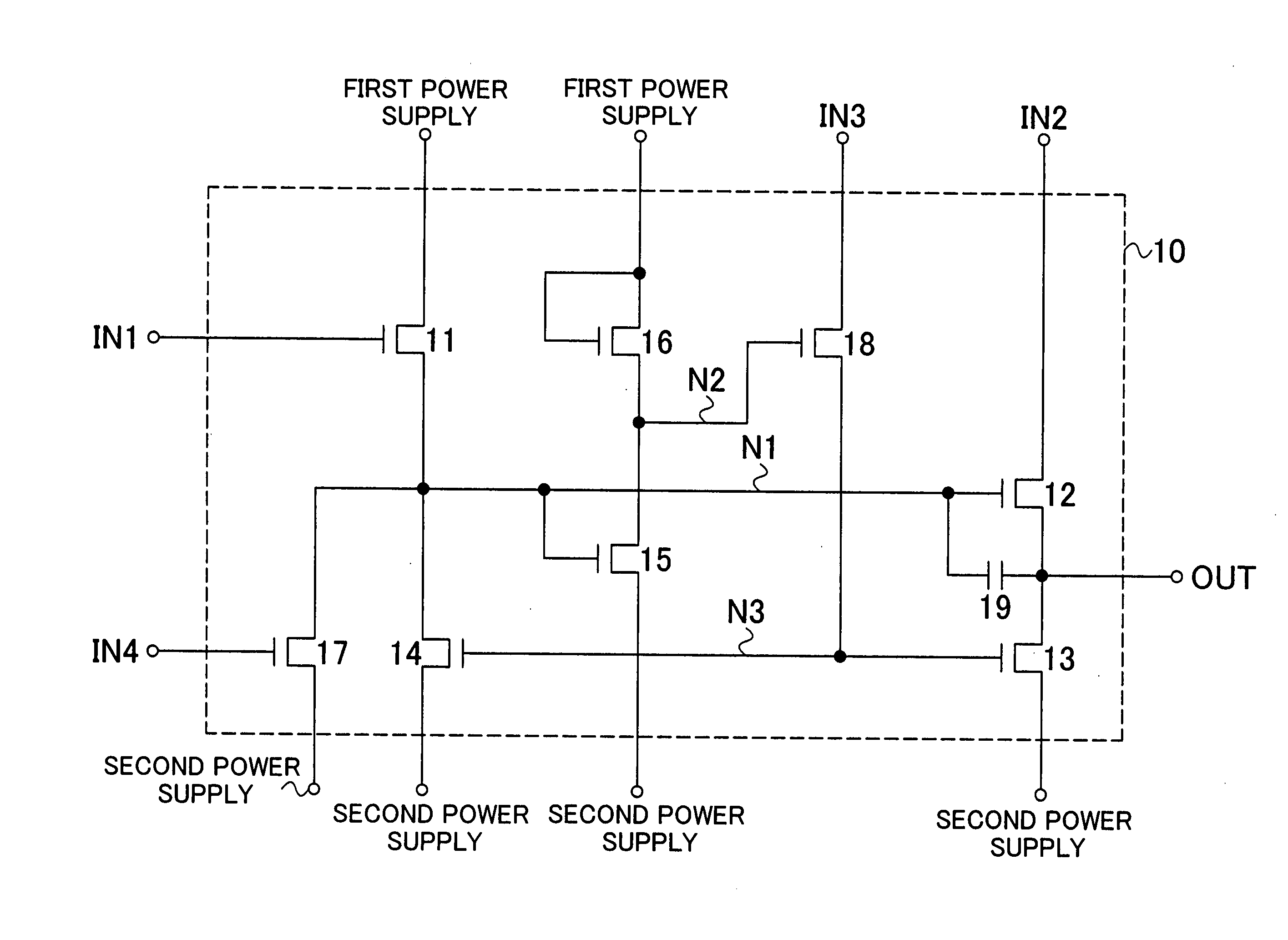
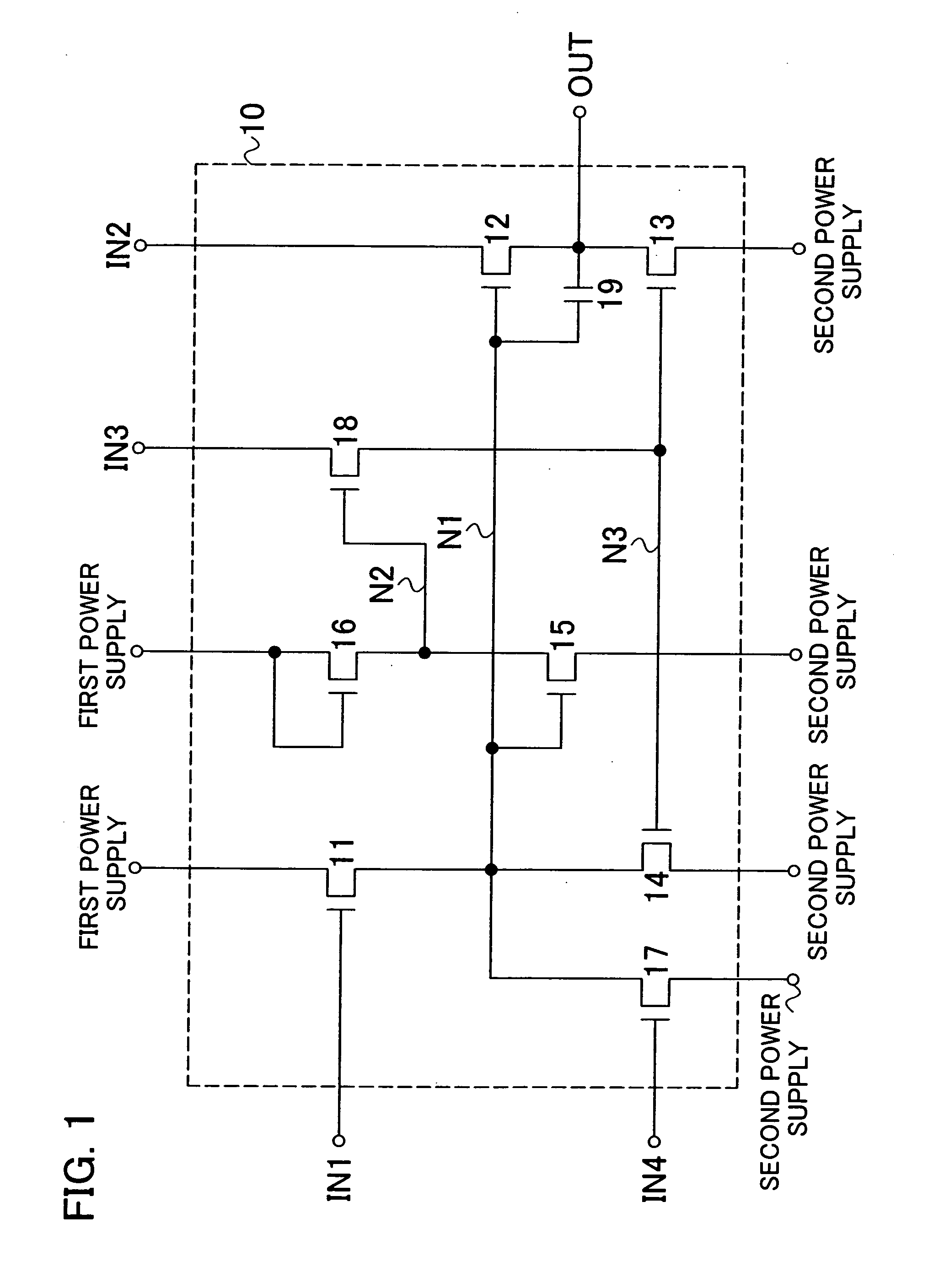
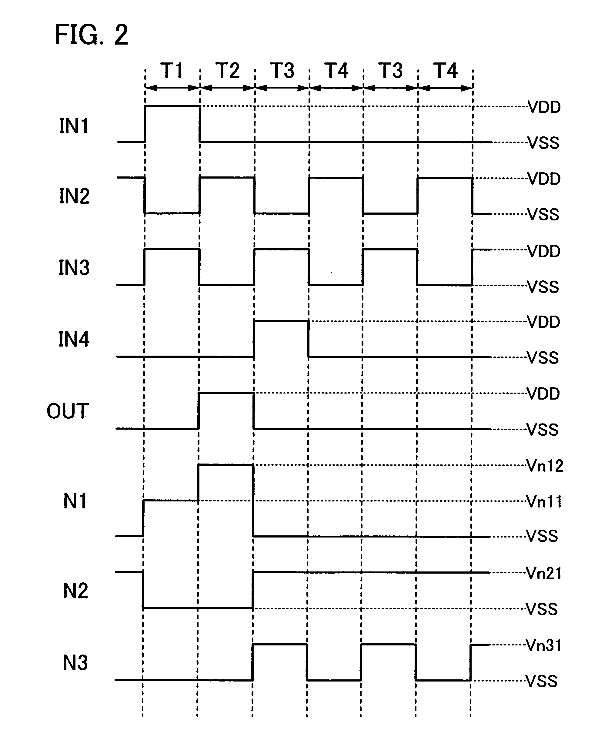
[0169]FIG. 1 shows one mode of a flip-flop circuit 10 of a shift register circuit of the invention. The shift register circuit of the invention includes a plurality stages of the flip-flop circuits 10. The flip-flop circuit 10 shown in FIG. 1 includes a transistor 11, a transistor 12, a transistor 13, a transistor 14, a transistor 15, a transistor 16, a transistor 17, a transistor 18, and a capacitor 19 having two electrodes. However, the capacitor 19 is not necessarily provided in the case where the gate capacitance of the transistor 12 can be used as the capacitor 19.

[0170]As shown in the flip-flop circuit 10, a gate terminal of the transistor 11 is connected to an input terminal IN1. A first terminal of the transistor 11 is connected to a first power supply. A second terminal of the transistor 11 is connected to a gate terminal of the transistor 12, a second terminal of the transistor 14, a gate terminal of the transistor 15, a second terminal of the transistor 17, and a second e...

embodiment mode 2

[0317]In this embodiment mode, a configuration of a shift register circuit of the invention is described.

[0318]FIG. 17 shows one mode of the shift register circuit of the invention. A shift register circuit shown in FIG. 17 includes a plurality of flip-flop circuits 171, a control signal line 172, a control signal line 173, and a control signal line 174.

[0319]As shown in the shift register circuit in FIG. 17, the input terminal IN1 in each of the flip-flop circuits 171 is connected to the output terminal OUT of a flip-flop circuit 171 in the previous stage. The output terminal OUT is connected to the input terminal IN1 of a flip-flop circuit 171 in the next stage, the input terminal IN4 of a flip-flop circuit 171 in the previous stage, and the output terminal SRout of the shift register circuit. Note that the input terminal IN1 of a flip-flop circuit 171 in a first stage is connected to the control signal line 172. In addition, the input terminal IN4 of a flip-flop circuit 171 in th...

embodiment mode 3

[0382]In this embodiment mode, a structure example in the case of using the flip-flop circuit described in Embodiment Mode 1, the shift register circuit described in Embodiment Mode 2, and the like as a part of a driver circuit is described.

[0383]A structure example of a driver circuit which can be applied to a gate driver is described with reference to FIGS. 20 to 27. Note that driver circuits in FIGS. 20 to 27 can be applied not only to gate drivers but also to any circuit structures.

[0384]FIG. 20 shows one mode of a gate driver of the invention. The gate driver of the invention includes a shift register circuit 200 and a buffer circuit 201.

[0385]As shown in the gate driver in FIG. 20, an output terminal SRout of the shift register circuit 200 is connected to an output terminal GDout of the gate driver through the buffer circuit 201.

[0386]Note that the shift register circuit 200 is similar to that described in Embodiment Mode 2.

[0387]In addition, output terminals SRout1 to SRout4 ...


PUM


Abstract

An object is to provide a semiconductor device which can suppress characteristic deterioration in each transistor without destabilizing operation. In a non-selection period, a transistor is turned on at regular intervals, so that a power supply potential is supplied to an output terminal of a shift register circuit. A power supply potential is supplied to the output terminal of the shift register circuit through the transistor. Since the transistor is not always on in a non-selection period, a shift of the threshold voltage of the transistor is suppressed. In addition, a power supply potential is supplied to the output terminal of the shift register circuit through the transistor at regular intervals. Therefore, the shift register circuit can suppress noise which is generated in the output terminal.

Description

TECHNICAL FIELD[0001]The present invention relates to a semiconductor device. In particular, the invention relates to a shift register which is formed by using transistors. In addition, the invention relates to a display device having the semiconductor device and an electronic device having the display device.BACKGROUND ART[0002]In recent years, since a large display device such as a liquid crystal television is increased, a display device such as a liquid crystal display device or a light-emitting device has been actively developed. In particular, a technique where a pixel circuit and a driver circuit including a shift register circuit or the like (hereinafter described as an internal circuit) are formed over the same substrate by using transistors which are formed by using an amorphous semiconductor over an insulator has been actively developed, since the technique greatly contributes to low power consumption and low cost. The internal circuit formed over the insulator is connecte...

Claims


Application Information

Patent Timeline
Patent Type & Authority Applications(United States)
IPC IPC(8): H03K3/356
CPCH03K3/356G02F1/13624G09G3/20G09G3/325G09G3/3266G09G3/3674G09G2300/0408G09G2300/0809G09G2310/0289G09G2310/0297G11C19/28H03K19/00369H03K19/003G09G3/36G09G2310/0286G09G3/3677G11C19/287H03K19/20H01L27/1214G09G3/3258G09G3/3696G09G2310/08G09G2330/021H01L27/124H03K3/356104
Inventor UMEZAKI, ATSUSHI
Owner SEMICON ENERGY LAB CO LTD
Why Eureka
Try Eureka