

High productivity combinatorial oxide terracing and pvd/ald metal deposition combined with lithography for gate work function extraction
- Summary
- Abstract
- Description
- Claims
- Application Information
AI Technical Summary
Benefits of technology
Problems solved by technology
Method used
Image

Examples
Embodiment Construction
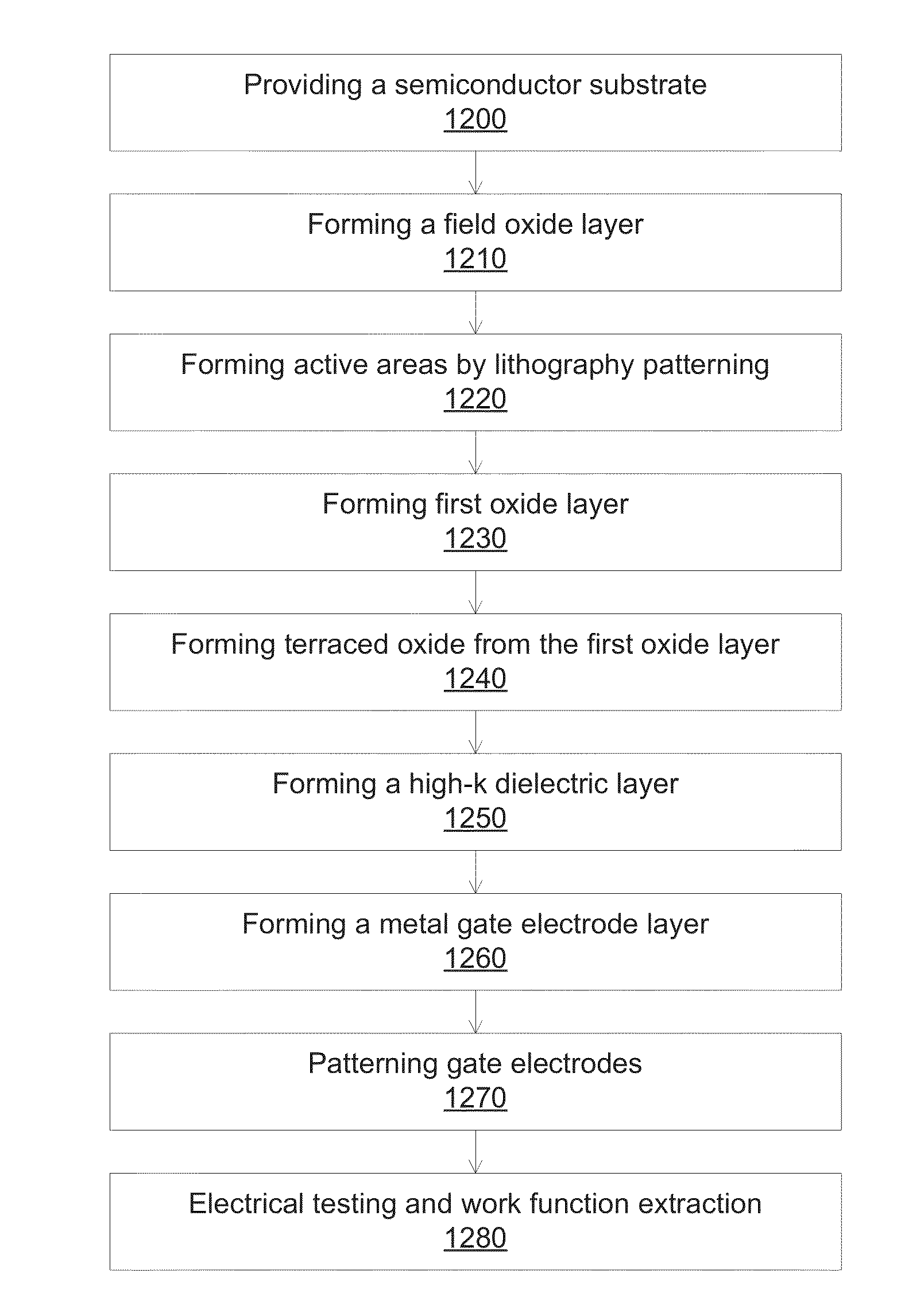
[0028]A detailed description of one or more embodiments is provided below along with accompanying figures. The detailed description is provided in connection with such embodiments, but is not limited to any particular example. The scope is limited only by the claims and numerous alternatives, modifications, and equivalents are encompassed. Numerous specific details are set forth in the following description in order to provide a thorough understanding. These details are provided for the purpose of example and the described techniques may be practiced according to the claims without some or all of these specific details. For the purpose of clarity, technical material that is known in the technical fields related to the embodiments has not been described in detail to avoid unnecessarily obscuring the description.
[0029]In some embodiments, the present invention discloses a combinatorial method to extract gate work function values from metal gate stacks including a metal electrode layer...
PUM
 Abstract
Description
Claims
Application Information