

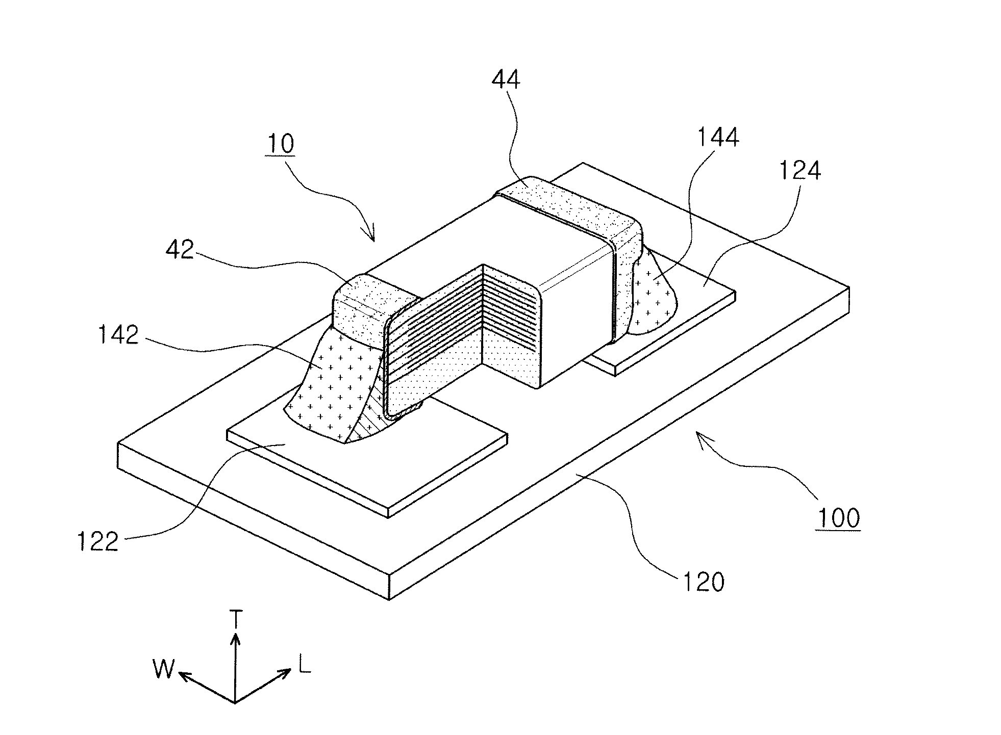
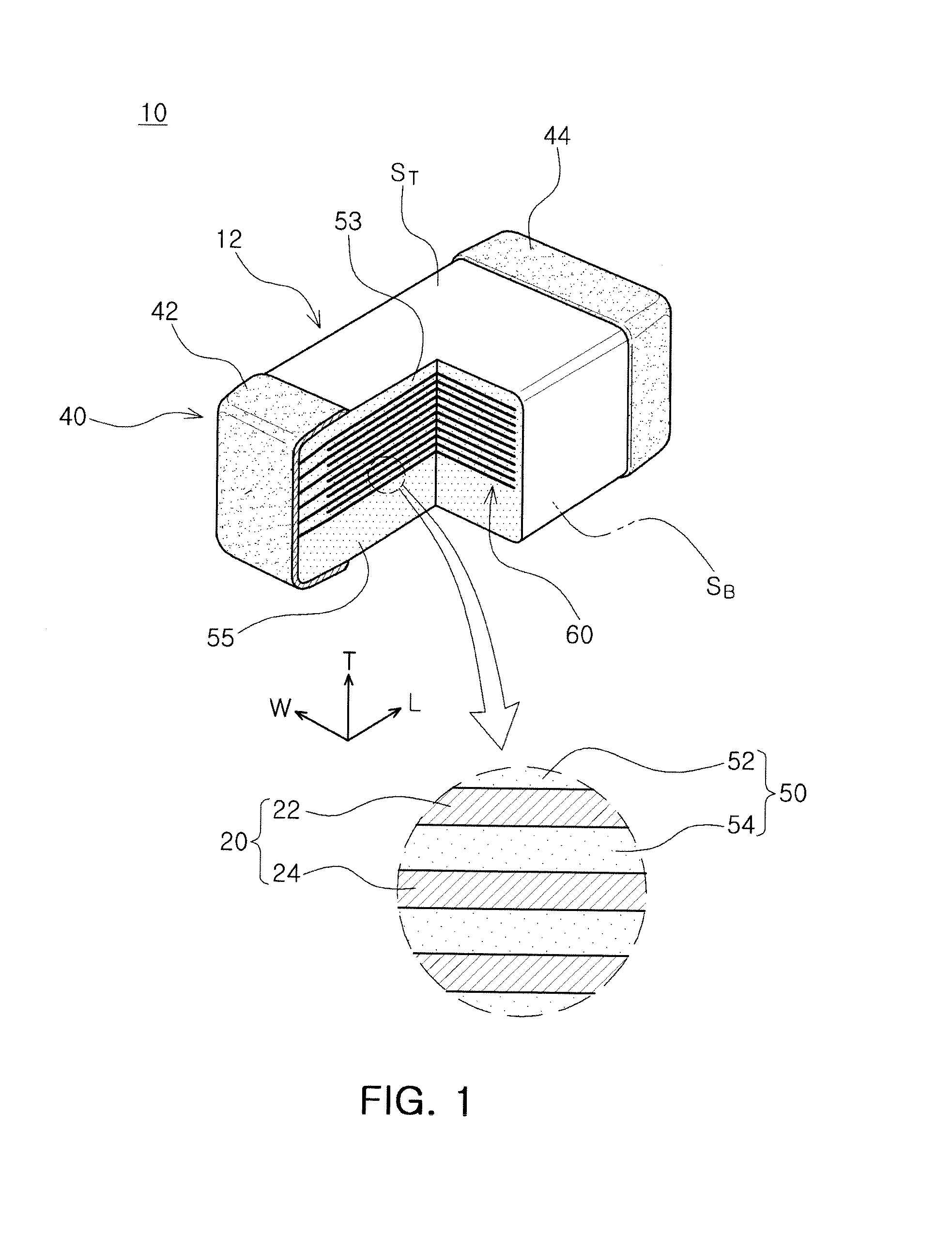
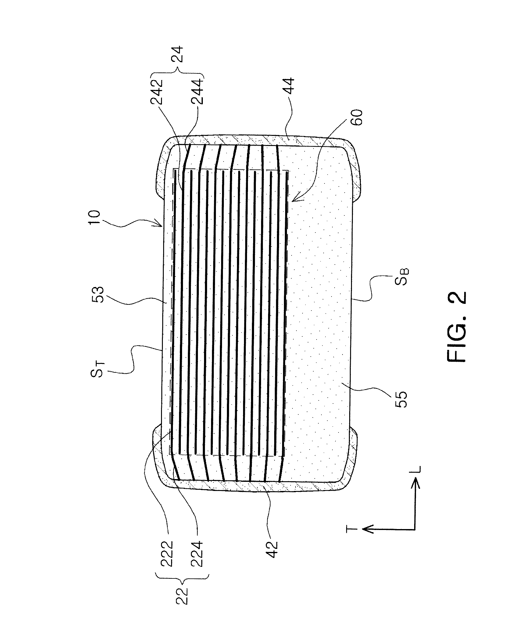
Laminated chip electronic component, board for mounting the same, and packing unit thereof
a technology for laminated chips and electronic components, applied in the direction of fixed capacitor details, printed circuit non-printed electric components association, final product manufacture, etc., can solve the problems of pcb vibrating to produce a noise, and user discomfort, and achieve the effect of reducing acoustic nois
- Summary
- Abstract
- Description
- Claims
- Application Information
AI Technical Summary
Benefits of technology
Problems solved by technology
Method used
Image

Examples
experimental example
[0119
[0120]Multilayer ceramic capacitors (MLCC) according to embodiments of the present invention and comparative examples were fabricated as follows.
[0121]The MLCCs according to the Examples were manufactured through the following steps.
[0122]First, slurry including powder such as barium titanate (BaTiO3), or the like, was applied to a carrier film and then dried to prepare a plurality of ceramic green sheets having a thickness of 1.8 μm.
[0123]Next, internal electrodes were formed by applying a conductive paste for a nickel internal electrode on the ceramic green sheets by using a screen.
[0124]About three hundreds and seventy (370) ceramic green sheets were laminated, and here, a larger number of ceramic green sheets without an internal electrode were laminated below ceramic green sheets with an internal electrode formed thereon than those above the ceramic green sheets with an internal electrode formed thereon. The laminate (or lamination body) was isostatic-pressed under a pressu...
PUM
| Property | Measurement | Unit |
|---|---|---|
| thickness | aaaaa | aaaaa |
| pressure | aaaaa | aaaaa |
| oxygen partial pressure | aaaaa | aaaaa |
Abstract
Description
Claims
Application Information