Magnetic field sensing device

a magnetic field and sensing device technology, applied in the direction of measurement devices, magnetic field magnitude/direction, instruments, etc., can solve the problems of significant amount of electric energy, low capacity of accumulaters, comparatively high electric energy consumption, etc., to reduce manufacturing complexity, high current, and large magnetic field

Inactive Publication Date: 2013-12-05
SENSITEC
View PDF9 Cites 24 Cited by
  • Summary
  • Abstract
  • Description
  • Claims
  • Application Information

AI Technical Summary

Benefits of technology

[0007]The invention suggests a magnetic field sensing device comprising several functionally different layers, wherein a Wheatstone bridge layer comprises at least two resistors of a Wheatstone bridge. Each resistor of the Wheatstone bridge comprises at least one magnetic field sensing element as a subresistor. A flip conductor layer comprises at least one flip conductor for flipping the internal magnetization state of each magnetic field sensing element. The flip conductor comprises a plurality of conductor stripes being arranged on at least two different flip conductor sublayers of said flip conductor layer, wherein the conductor stripes of the sublayers are electrically coupled with each other through via connections, i.e. so-called vias. Thus, the magnetic field sensing device suggests a design of a sensor chip, wherein the flip conductor is arranged on at least two sublayers which can lie on top of each other or which may sandwich the Wheatstone resistors. Such a design requires nearly half the size of a conventional magnetic sensor chip area. This results from the multilayered structure of the flip conductor being arranged on at least two sublayers. The three-dimensional structure reduces chip size outside of the area, where the magnetic field sensing elements are located, thus making the overall size of the sensor chip more compact. Furthermore, due to the compact design, magnetic stray fields can be decreased and inductance can be reduced. The magnetically active conductor stripes adjacent to the magnetic field sensing elements can be designed with a U-shape, a meandering shape or a spiral shape and can exert equivalent or superior effects on the flipping mechanism as existing flip conductor structures. The basic concepts of the flipping mechanism follow conventional designs, i.e. flipping the orientation of the magneto-resistive stripes of each resistor relative to the conductor stripes of a flip conductor sublayer close to the magnetic sensing elements. As a result, the magnetic field sensing elements of the resistor arrangement can be located more closely to each other, such that magnetic field sensing elements are rendered more homogeneous and material impurities and fabrication defects affect two or more resistors equally, resulting in the following improvements:
[0028]In general, a single flip conductor is provided for simultaneously flipping all magnetic field sensing elements of the Wheatstone bridge. According to a preferred embodiment, two or more electrically separated flip conductors for independently flipping a magnetization state of at least one magnetic field sensing element of a bridge resistor can be provided. Two independent flip conductors allow the independent flipping of half of the magnetic field sensing elements. Both flip conductors can generate four different flip states of the magnetic field sensing elements of a Wheatstone bridge resistor, such that the sensitivity of the Wheatstone bridge can be switched on or off. This allows the measuring of the offset voltage of the bridge, as well as performing a self-test of the bridge. The offset voltage can be used to further improve accuracy of the magnetic field sensing device.

Problems solved by technology

Many electric devices incorporating a magnetic field sensor chip are powered by batteries or accumulators with low capacity.
Arranging a comparatively large flip conductor on a single layer of a sensor chip results in a comparatively high electric energy consumption in the generation of a sufficiently large magnetic flipping field for flipping the internal magnetization of the magnetic field sensing elements, occupies a large part of the chip area, consumes a significant amount of electric energy and exhibits a high inductance, such that only comparatively low flipping frequencies can be attained which limit the temporal resolution of the magnetic field sensing.
A problem encountered with the magnetic field sensing devices known from the state of the art resides in the aspect that the magnetic field conductor is relatively large with respect to the AMR resistor configuration, consumes a relatively high amount of electric energy and does not allow to increase a flipping frequency, such that a higher miniaturization and better resolution of the magnetic field sensing device is limited.

Method used


Image

  • Magnetic field sensing device
  • Magnetic field sensing device
  • Magnetic field sensing device

Examples


first embodiment

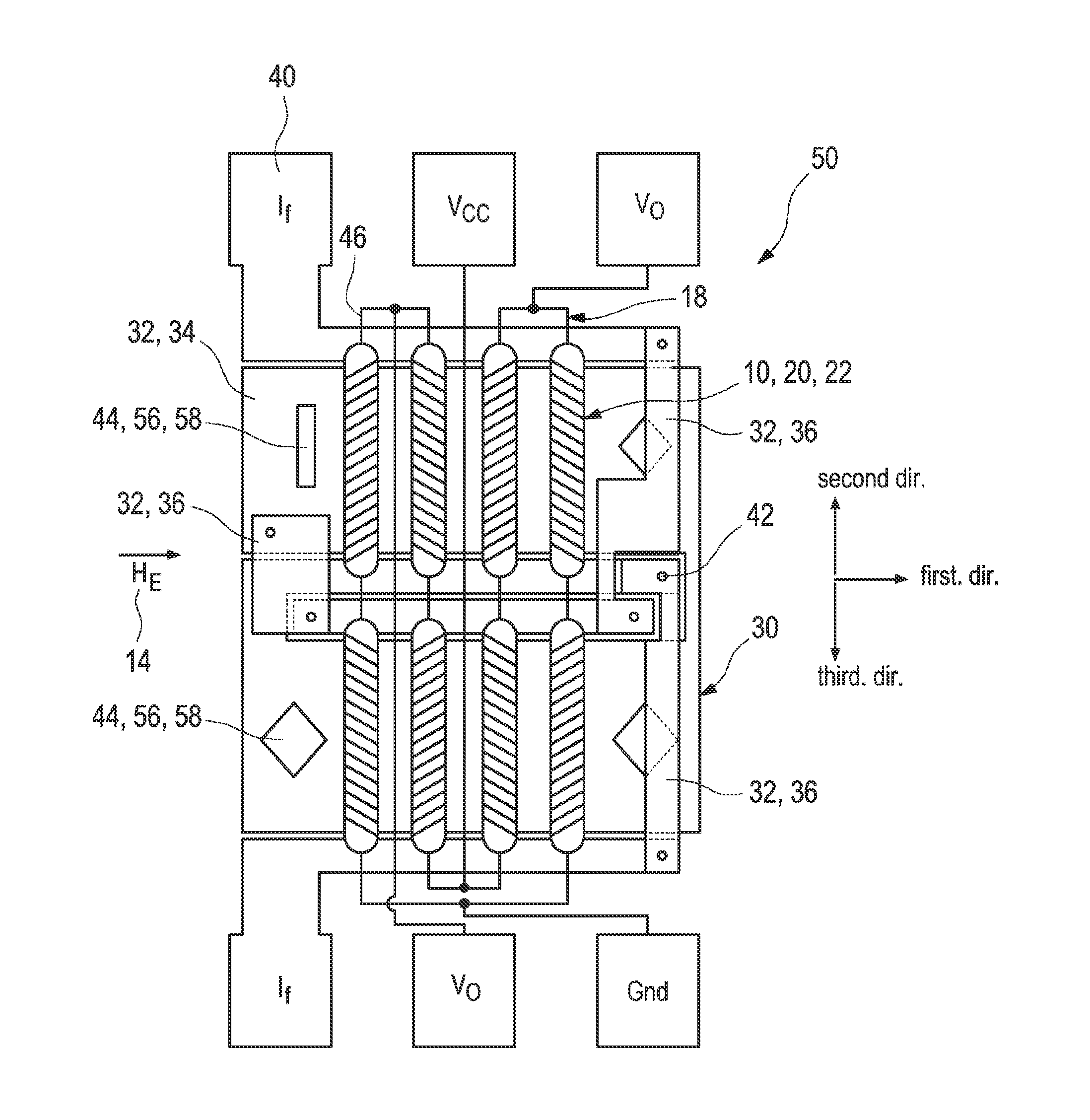
[0056]FIG. 6 shows a magnetic field sensing device 50 according to the invention. The magnetic field sensor chip 50 comprises a Wheatstone bridge 18, wherein each bride resistor 20 comprises two subresistors 22, which are designed as magnetic field sensing elements 10 with alternating Barberpole structures 16, 26, 28. The Wheatstone bridge 18 is arranged on a first layer of the device 50. The Wheatstone bridge 18 is connected to four contacting pads 40 for supplying the Wheatstone bridge 18 with electric energy Vcc, Gnd and for sensing a voltage difference ΔVo from pads Vo as a result of an external magnetic field HE 14. The Wheatstone bridge 18 is arranged on top of a flip conductor layer 38, which comprises two sublayers 38-1 and 38-2.

[0057]A detailed drawing of the individual sublayers is depicted in FIG. 7a to FIG. 7c. A flip conductor 30 is arranged on a flip conductor layer 30 and can be contacted by contacting pads 40, for feeding a flipping current pulse IF into the conducto...

second embodiment

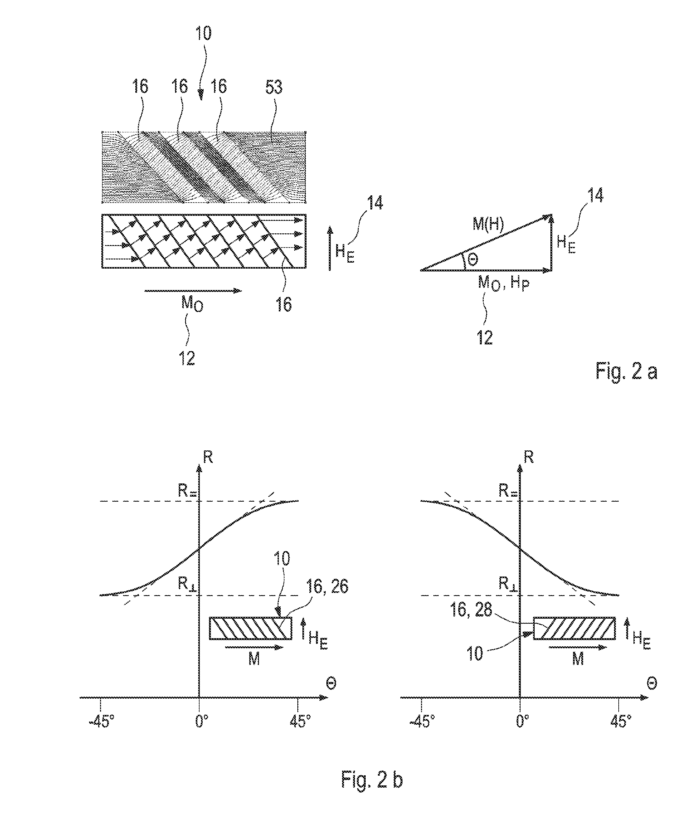
[0059]FIG. 8 displays a magnetic field sensing device 50 with an interdigital arrangement 24 of bridge resistors 20. The flip conductor arrangement 30 is similar to the flip conductor of the embodiment depicted in FIGS. 6, 7. The Wheatstone bridge 18 comprises four resistors 20, whereby each resistor 20 comprises a plurality of magnetic field sensing elements 10 in the form of subresistors 22. The magnetic field sensing elements 10 of each resistor 20 are series-connected, whereby two sensing elements 10 with alternating Barberpole structures 26, 28 are arranged on magnetically active conductor stripes 32 of the first sublayer 38-1 of the flip conductor 30 generating opposing magnetic flipping fields Hflip. The series-connected elements 10 of each resistor 20 are arranged in a meandering form, such that interdigitating fingers are formed. The fingers of two resistors 20 interact such that the bridge resistors 20 are formed in an interdigital arrangement 24, wherein magnetic elements...


PUM


Abstract

The present invention relates to a magnetic field sensing device (50) comprising several functionally different layers (38, 60, 70), wherein a Wheatstone bridge layer (70) comprises at least two resistors (20) of a Wheatstone bridge (18), each resistor (20) comprises at least one magnetic field sensing element (10) in the form of a resistor subelement (22), and a flip conductor layer (38) comprising at least one flip conductor (30) for flipping the internal magnetization state of each magnetic field sensing element (10). The flip conductor (30) comprises a plurality of conductor stripes (32) being arranged on at least two different flip conductor sublayers (38-1, 38-2) of said flip conductor layer (38) and being electrically coupled with each other through vias.The multilayer arrangement of said flip conductor (30) provides a compact design of said magnetic field sensing device (50), such that a decreased power consumption, decreased inductance and improved sensitivity of the magnetic field sensing device can be achieved.

Description

TECHNICAL FIELD[0001]The present invention relates to a magnetic field sensing device for sensing a direction and magnitude of an external magnetic field.BACKGROUND ART[0002]The AMR effect (Anisotropic Magneto Resistance Effect) is used in a wide array of sensors, especially for the measurement of the earth's magnetic field, as an electronic compass or for electric current measurement (by measuring the magnetic field created around the conductor), for traffic detection and for linear position sensing and angle sensing. Typically, AMR magnetic field sensing devices comprise magnetic field sensing elements utilizing the AMR effect, which is the property of a conductive material to change the value of its electrical resistance when an external magnetic field is applied. Using a Wheatstone bridge configuration enables a highly sensitive measurement of resistance variations of the AMR sensitive bridge resistors. Since more and more highly compact electronic devices, such as navigation sy...

Claims


Application Information

Patent Timeline
Patent Type & Authority Applications(United States)
IPC IPC(8): G01R33/09
CPCG01R33/096B82Y25/00G01R31/318516G01R33/0011G01R33/0017G01R33/093G01R33/098
Inventor LOREIT, UWEWEBER, SEBASTIAN
Owner SENSITEC
Why Eureka
Try Eureka