Semiconductor device

a semiconductor device and semiconductor technology, applied in the direction of semiconductor devices, basic electric elements, electrical equipment, etc., can solve the problems of insufficient high-efficiency field plate structure to achieve high-efficiency breakdown voltage performance, etc., to achieve the effect of improving the breakdown voltage, relaxing the electric field, and reducing the concentration of electric fields

Active Publication Date: 2013-12-12
TOYODA GOSEI CO LTD
View PDF9 Cites 15 Cited by
  • Summary
  • Abstract
  • Description
  • Claims
  • Application Information

AI Technical Summary

Benefits of technology

[0028]According to the present invention, in the vicinity of the pn junction interface exposed on the side surface of the step, a sufficiently large electric field relaxing region cannot be formed, and the concentration of the electric field is reduced, thereby further improving the breakdown voltage.
[0029]According to the second aspect of the present invention, the depth of the step and the thickness of the protective film can be appropriately set, thereby achieving a high breakdown voltage performance.
[0030]According to the third aspect of the present invention, the breakdown voltage can be further improved.
[0031]According to the fourth aspect of the present invention, the concentration of the electric field at the bottom edge of the step can be reduced, thereby further improving the breakdown voltage.
[0032]As in the fifth aspect of the present invention, the breakdown voltage of the device can be further improved by changing the thickness of the protective film at forming locations.

Problems solved by technology

When a reverse voltage is applied, a large electric field is concentrated at the end of this pn junction interface, causing a problem that the breakdown voltage of the semiconductor device does not reach the design value.
However, the field plate structure suitable for high breakdown voltage, e.g. the thickness of the protective film or the depth of the step is not deeply considered in Non-patent Document 1 and Patent Document 1.
Just employing the field plate structure is not enough to achieve a high breakdown voltage performance as designed.

Method used


Image

  • Semiconductor device
  • Semiconductor device
  • Semiconductor device

Examples


embodiment 1

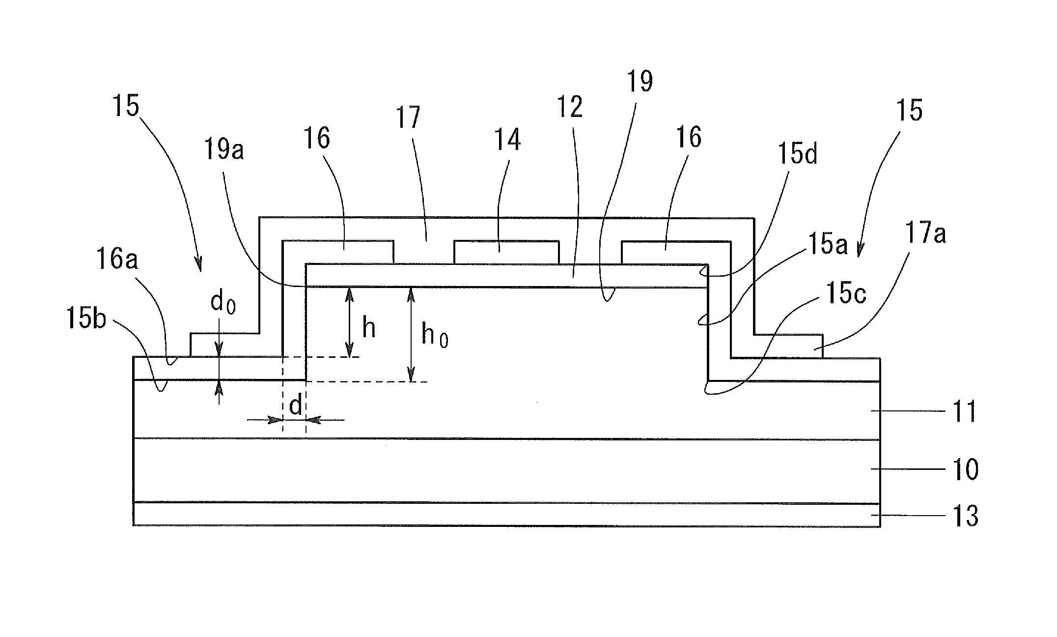
[0042]FIG. 1 shows the configuration of a vertical diode according to Embodiment 1. The vertical diode according to Embodiment 1 comprises a substrate 10, an n-layer 11 disposed on the substrate 10, and a p-layer 12 disposed on the n-layer 11 as shown in FIG. 1. An n-electrode 13 is formed in contact with the substrate 10 on the surface opposite the surface of the substrate 10 on which the p-layer 11 is formed, and a p-electrode 14 is formed on a portion of the p-layer 12. The vertical diode according to Embodiment 1 has a field plate structure comprising a protective film 16 and a field plate electrode 17. The vertical diode according to Embodiment 1 is a circle in plan view, whose diameter is 200 μm. The shape in plan view is not limited to a circle, and may be a rectangle. In case of a rectangle, the corners are preferably rounded, thereby improving the breakdown voltage performance.

[0043]The substrate 10 comprises n-GaN. A substrate of any material other than n-GaN may be used, ...

embodiment 2

[0073]FIG. 7 shows the configuration of a vertical trench gate MOSFET according to Embodiment 2. The vertical trench gate according to Embodiment 2 comprises a substrate 20, an n-layer 21 of n-GaN formed on the substrate 20, a p-layer 22 of p-GaN formed on the n-layer 21, and a high concentration n-layer 23 of n-GaN formed on the p-layer 22. It also has a trench gate. That is, a trench 24 extending from the surface of the high concentration n-layer 23 (the surface opposite the surface of the p-layer 22) through the p-layer 22 to the n-layer 21 is formed. A gate insulating film 25 is formed so as to continuously cover the vicinity of an opening of the trench 24 on the surface of the n-layer 23, a side surface and a bottom surface of the trench 24. A gate electrode 26 is formed in contact with the gate insulating film 25 inside the trench 24.

[0074]On the surface of the high concentration n-layer 23, a trench 27 is formed so as to reach the p-layer 22, and a source electrode 28 is prov...


PUM


Abstract

A device comprises a substrate, an n-layer and a p-layer, an n-electrode, and a p-electrode. A step is formed at an outer circumference of the device. A protective film is formed so as to continuously cover a side surface and a bottom surface of the step. A field plate electrode connected with the p-electrode is formed on the protective film. When a distance from the pn junction interface to the surface of the protective film on the bottom surface of the step is defined as h (μm), a dielectric constant of the protective film is defined as ∈s, and a thickness of the protective film at the pn junction interface on the side surface of the step is defined as d (μm), (∈s·h)/d is 4 or more, and ∈s/d is 3 (1/μm) or more.

Description

BACKGROUND OF THE INVENTION[0001]1. Field of the Invention[0002]The present invention relates to a vertical semiconductor device having a field plate structure, particularly characterized by the thickness of the protective film in the field plate structure and the depth of the step.[0003]2. Background Art[0004]Semiconductor devices such as diode or FET can be classified into two types by its structure: a vertical type which establishes electrical continuity in a direction perpendicular to the main surface and a horizontal type which establishes electrical continuity in a direction parallel to the main surface. The vertical type has more advantages such as high breakdown voltage or improved area efficiency than the horizontal type. In the vertical semiconductor device having a pn junction structure, a pn junction interface is exposed on the side surface of the step. When a reverse voltage is applied, a large electric field is concentrated at the end of this pn junction interface, cau...

Claims


Application Information

Patent Timeline
Patent Type & Authority Applications(United States)
IPC IPC(8): H01L29/78H01L29/861
CPCH01L29/7827H01L29/861H01L29/0661H01L29/2003H01L29/407H01L29/41741H01L29/41766H01L29/517H01L29/518H01L29/7811H01L29/7813H01L29/8613
Inventor UENO, YUKIHISAOKA, TORU
Owner TOYODA GOSEI CO LTD
Why Eureka
Try Eureka