Circuit sharing time delay integrator

Inactive Publication Date: 2013-12-19
NAT APPLIED RES LAB
0 Cites 0 Cited by

AI-Extracted Technical Summary

Problems solved by technology

However, its most notable drawback is that the quantity of required circuits increases with the quantity of the signals to be accumulated and thus, in practice, the circuits are s...

Benefits of technology

[0010]1. Reduce the quantity of operational amplifiers or load circuits, and lessen the complexity of the time delay integrator circuit structure.
[0011]2. Enable a great reduction in ...

Abstract

The present invention discloses a circuit sharing time delay integrator structure. The major composing elements of this circuit sharing time delay integrator structure are: a sharing circuit, a first control block, a plurality of second control blocks and a timing set generated by a timing generator circuit. The sharing circuit can be an OP-AMP, an active load, or any of a variety of combinations used in signal accumulation applications. With the implementation of the present invention to applications of signal accumulations, the necessity of an adder circuitry is eliminated, the overall circuitry and hence the total amount of transistors required when producing the integrated circuit is massively reduced, and thus a great cost reduction and better timing and power efficiency can all be thereof achieved.

Application Domain

Computing operations for integral formationComputing operations for integration/differentiation +1

Technology Topic

IntegratorTiming generator +5

Image

  • Circuit sharing time delay integrator
  • Circuit sharing time delay integrator
  • Circuit sharing time delay integrator

Examples

  • Experimental program(1)

Example

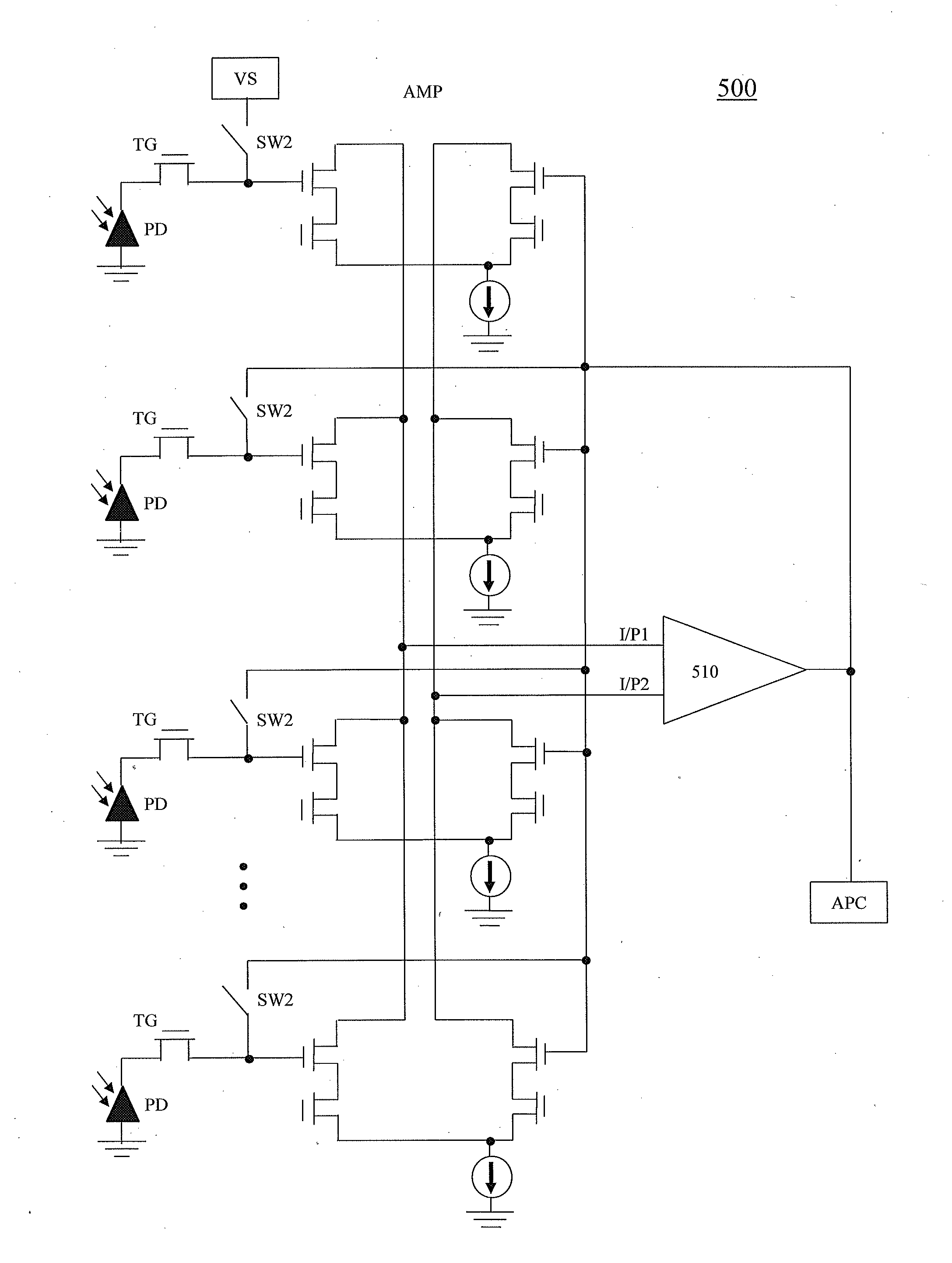
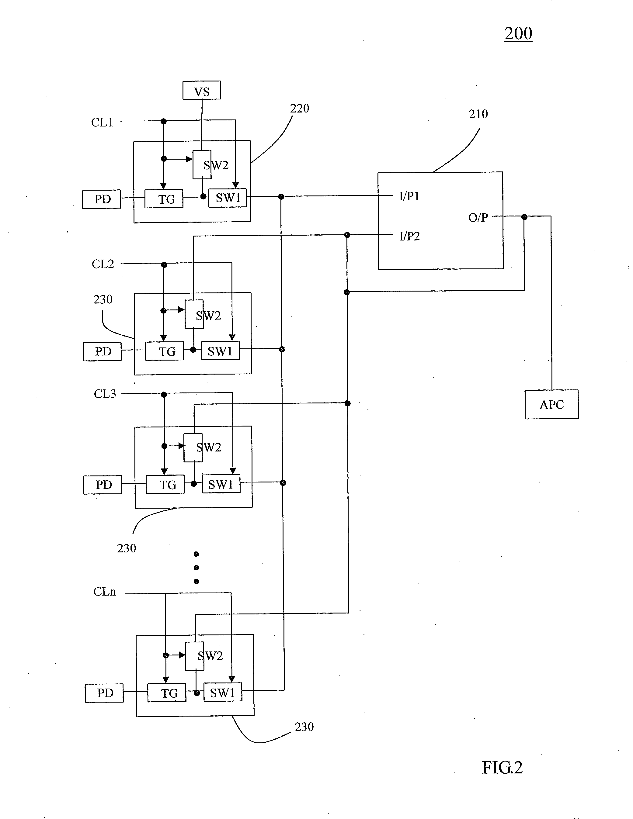
[0021]FIG. 2 is a circuit diagram of a time delay integrator structure 200 having a shared feedback type operational amplifier circuit 210 according to an embodiment of the present invention. FIG. 3 is a schematic view of clock signals 300 (CL1˜CLn) generated by a set of clock signals according to an embodiment of the present invention. FIG. 4 and FIG. 5 are circuit diagrams of time delay integrator structures 400, 500 equipped with shared active load circuit modules 410, 510. FIG. 6 is a circuit diagram of implementation of the time delay integrator structure 200 having the shared feedback type operational amplifier circuit 210 according to an embodiment of the present invention. FIG. 7 and FIG. 8 are circuit diagrams of implementation of the time delay integrator structures 400, 500 equipped with shared active load circuit modules according to an embodiment of the present invention.
[0022]Referring to FIG. 2, FIG. 4, and FIG. 5, the present invention provides circuit sharing time delay integrator structures 200, 400, 500 comprising: a sharing circuit provided in the form of the feedback type operational amplifier circuit 210, the active circuit module 410, or the active load circuit module 510; a first control block 220, a third control block 420, or a fifth control block 520; a plurality of second control blocks 230, fourth control blocks 430, or sixth control blocks 530; and the clock signals 300 (CL1˜CLn).
[0023]Referring to FIG. 2, there is shown the circuit structure 200 of a circuit sharing time delay integrator of the present invention, comprising the feedback type operational amplifier circuit 210, the first control block 220, the plurality of second control blocks 230, and the clock signals 300. The feedback type operational amplifier circuit 210 has a first input end I/P1, a second input end I/P2, and an output end O/P, and effectuates feedback by electrical connection of the second input end I/P2 and the output end O/P.
[0024]The first control block 220 comprises a transfer gate TG and a first switch SW1 which are connected in series to the first input end I/P1. An input end of the transfer gate TG is connected in series to a photo detector PD. The first control block 220 comprises a second switch SW2. One end of the second switch SW2 is electrically connected between the transfer gate TG and the first switch SW1, and the other end of the second switch SW2 is electrically connected to a reset voltage source VS. The reset voltage source VS serves as an initial voltage source for the circuit structure 200 of the circuit sharing time delay integrator in its entirety.
[0025]The second control blocks 230 each comprises a transfer gate TG and the first switch SW1 that are connected in series to the first input end I/P1. An input end of the transfer gate TG is connected in series to a photodetector PD. The second control blocks 230 each comprises a second switch SW2. One end of the second switch SW2 is electrically connected between the first switch SW1 and the transfer gate TG in the second control blocks 230, and the other end of the second switch SW2 is electrically connected to the second input end I/P2.
[0026]In the circuit structure 200 of the circuit sharing time delay integrator of the present invention, the feedback type operational amplifier circuit 210 is shared by the first control block 220 and the second control blocks 230, thereby serving as the sharing circuit of the present invention.
[0027]The clock signals 300 (CL1˜CLn) provide a set of clocks required for the operation of the time delay integrator. First, the clock signals 300 (CL1˜CLn) trigger an ON state in the first control block 220. Then, the clock signals 300 (CL1˜CLn) trigger ON states in the second control blocks 230 in sequence. Signals received by a photo detector PD are accumulated in every instance of triggering an ON state. After the signals of every photo detectors PD have been accumulated by the circuit structure 200 of the circuit sharing time delay integrator of the present invention, the final total output is effectuated by a back-end processing circuit APC. The conducting state and the cut off state of the clock signals are denoted by ON and OFF, respectively.
[0028]Referring to FIG. 4, in another embodiment of the present invention, the circuit structure 400 of the circuit sharing time delay integrator comprises the active circuit module 410, the third control block 420, the fourth control blocks 430, and the clock signals 300. The active circuit module 410 comprises a constant current source, a negative end input unit, and a load unit of a feedback type amplifying circuit, and has a first input end I/P1, a second input end I/P2, and an output end O/P. The active circuit module 410 effectuates feedback by electrical connection of the second input end I/P2 and the output end O/P.
[0029]The third control block 420 comprises a transfer gate TG and a source follower unit DF that are connected in series to the first input end I/P1. An input end of the transfer gate TG is connected in series to a photo detector PD. The third control block 420 further comprises a second switch SW2. One end of the second switch SW2 is electrically connected between the transfer gate TG and the source follower unit DF, and the other end of the second switch SW2 is electrically connected to the reset voltage source VS. The reset voltage source VS serves as an initial voltage source for the circuit structure of the circuit sharing time delay integrator in its entirety.
[0030]The fourth control blocks 430 each comprises a transfer gate TG and a source follower unit DF that are connected in series to the first input end I/P1. An input end of the transfer gate TG is connected in series to a photo detector PD. The fourth control blocks 430 each comprise a second switch SW2. One end of the second switch SW2 is electrically connected between the transfer gate TG and the source follower unit DF, and the other end of the second switch SW2 is electrically connected to the second input end I/P2.
[0031]The clock signals 300 (CL1˜CLn) trigger an ON state in the third control block 420, and then trigger ON states in the fourth control blocks 430 in sequence. Signals received by a photo detector PD are accumulated in every instance of triggering an ON state. After the signals of every photo detectors PD have been accumulated by the circuit structure 400 of the circuit sharing time delay integrator of the present invention, the final total output is effectuated by the back-end processing circuit APC. The conducting state and cut off state of the clock signals are denoted by ON and OFF, respectively.
[0032]Referring to FIG. 5, in another embodiment of the present invention, the circuit structure 500 of the circuit sharing time delay integrator comprises an active load circuit module 510, the fifth control block 520, the plurality of sixth control blocks 530, and the clock signals 300. The active load circuit module 510 is a load unit of a feedback amplifying circuit and has a first input end I/P1, a second input end I/P2, and an output end O/P. The second input end I/P2 is electrically connected to the output end O/P, thereby providing a path of signal transmission to the next level.
[0033]The fifth control block 520 comprises a transfer gate TG and an amplifier circuit AMP that are connected in series to the first input end I/P1. An input end of the transfer gate TG is connected in series to a photo detector PD. The fifth control block 520 further comprises a second switch SW2. One end of the second switch SW2 is electrically connected between the transfer gate TG and the amplifier circuit AMP, and the other end of the second switch SW2 is electrically connected to the reset voltage source VS. The reset voltage source VS serves as an initial voltage source for the circuit structure of the circuit sharing time delay integrator in its entirety.
[0034]The sixth control blocks 530 each comprises a transfer gate TG and an amplifier circuit AMP that are connected in series to the first input end I/P1. An input end of each said transfer gate TG is connected in series to a photo detector PD. The sixth control blocks 530 each comprise a second switch SW2. One end of the second switch SW2 is electrically connected between the transfer gate TG and the amplifier circuit AMP, and the other end of the second switch SW2 is electrically connected to the second input end I/P2.
[0035]The clock signals 300 (CL1˜CLn) trigger an ON state in the fifth control block 520, and then trigger ON states in the sixth control blocks 530 in sequence. In the circuit structure 500 of the circuit sharing time delay integrator, the active load circuit module 510 is shared by the fifth control block 520 and the sixth control blocks 530. After the signals of every photo detectors PD have been accumulated by the circuit structure 500 of the circuit sharing time delay integrator of the present invention, the final total output is effectuated by the back-end processing circuit APC. The conducting state and cut off state of the clock signals are denoted by ON and OFF, respectively.
[0036]The embodiments described above are only the preferred embodiments of, but not limitations to, the present invention. While the present invention is disclosed herein with reference to the preferred embodiments, the embodiments are not intended to restrict the present invention. Based on the technical contents disclosed herein, a person skilled in the art may alter or modify the foregoing embodiments and thereby produce equivalent embodiments without departing from the scope of the present invention. Therefore, all minor alterations and equivalent changes which are based on the technical substance of the present invention and made to the foregoing embodiments should be considered as within the scope of the technical solution of the present invention.

PUM

no PUM

Description & Claims & Application Information

We can also present the details of the Description, Claims and Application information to help users get a comprehensive understanding of the technical details of the patent, such as background art, summary of invention, brief description of drawings, description of embodiments, and other original content. On the other hand, users can also determine the specific scope of protection of the technology through the list of claims; as well as understand the changes in the life cycle of the technology with the presentation of the patent timeline. Login to view more.

Similar technology patents

Classification and recommendation of technical efficacy words

Why Eureka
Try Eureka