Transistor with recess gate and method for fabricating the same

a technology of transistor and recess gate, which is applied in the direction of semiconductor devices, basic electric elements, electrical apparatus, etc., can solve the problems of increasing leakage current of memory cells, deteriorating refresh characteristics, and a high probability of penetration phenomenon, so as to improve the doping efficiency of the recess gate structure

Active Publication Date: 2014-01-02
SK HYNIX INC
View PDF8 Cites 8 Cited by
  • Summary
  • Abstract
  • Description
  • Claims
  • Application Information

AI Technical Summary

Benefits of technology

[0013]Embodiments of the present invention are directed to a transistor having an improved doping efficiency of a recess gate structure, and a method for fabricating the same.

Problems solved by technology

In particular, if the short channel effect occurs in a cell transistor, which is adopted in the memory cell of a DRAM, leakage current of the memory cell increases, and a refresh characteristic deteriorates.
However, in the ion beam implantation method, a problem may be caused in that a penetration phenomenon is likely to occur as indicated by the reference symbols {circle around (2)} and {circle around (3)}.
Therefore, in the recess gate structure, while doping may be sufficiently performed on the surface and up to an intermediate zone {circle around (4)}, it is difficult to sufficiently perform doping up to a deep zone {circle around (5)} of a recess.

Method used


Image

  • Transistor with recess gate and method for fabricating the same
  • Transistor with recess gate and method for fabricating the same
  • Transistor with recess gate and method for fabricating the same

Examples


first embodiment

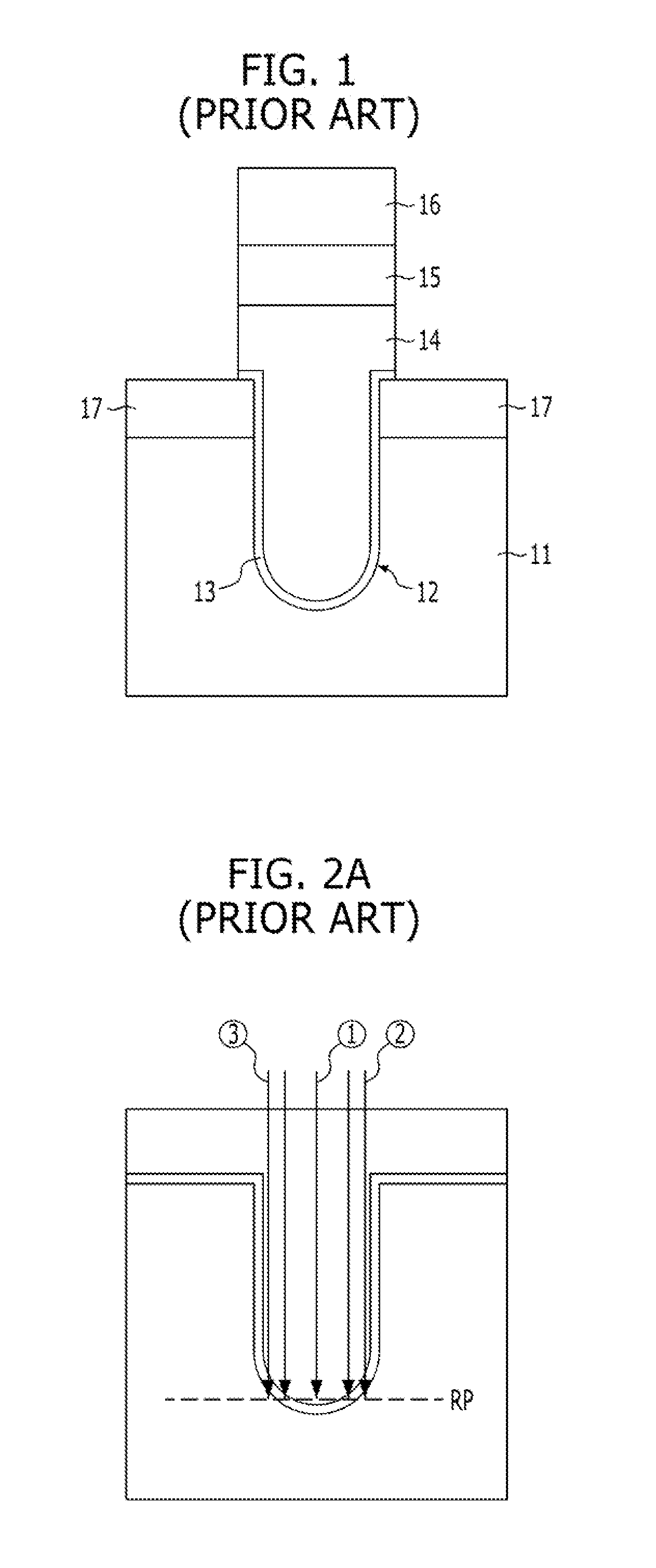
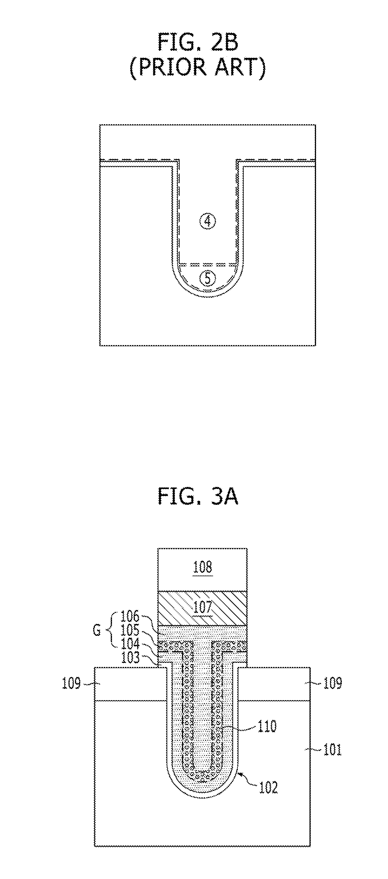
[0034]FIG. 3A is a view illustrating a transistor with a recess gate structure in accordance with the present invention.

[0035]Referring to FIG. 3A, a recess 102 is defined in a semiconductor substrate 101. A gate dielectric layer 103 is formed on the surface of the semiconductor substrate 101 that defines the recess 102. A silicon-containing electrode G is formed on the gate dielectric layer 103 to fill the recess 102. The silicon-containing electrode G may project out of the surface of the semiconductor substrate 101 while filling the recess 102. A metal electrode 107 and a gate hard mask layer 108 are formed on the silicon-containing electrode G. Source / drain regions 109 are formed in the semiconductor substrate 101 on both sides of the silicon-containing electrode G.

[0036]In FIG. 3A, as the silicon-containing electrode G, a lower layer, an intermediate layer and an upper layer may be stacked. For example, the lower layer, the intermediate layer and the upper layer respectively in...

second embodiment

[0070]FIG. 5 is a view illustrating a transistor with a recess gate structure in accordance with the present invention.

[0071]Referring to FIG. 5, a semiconductor substrate 201 has a plurality of transistor regions. The plurality of transistor regions may include a first region and a second region. An isolation region 202 is formed to isolate the first region and the second region from each other. The isolation region 202 has a trench structure and may be formed through an STI (shallow trench isolation) process. The isolation region 202 may include a dielectric layer (for example, a silicon oxide). The first region is a region where an NMOS is formed, and the second region is a region where a PMOS is formed. Hereinafter, the first region and the second region will be referred to as the “first NMOS region” and the “second PMOS region,” respectively. The positions of the first NMOS region and the second PMOS region are for the sake of convenience in explanation, and may be interchanged...

third embodiment

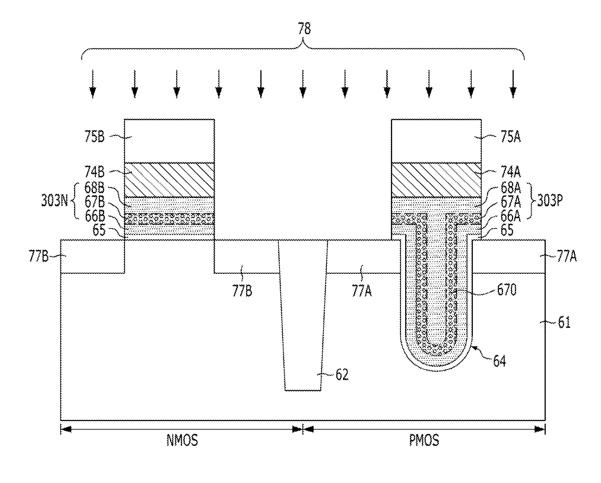
[0114]FIG. 7 is a view illustrating a transistor with a recess gate structure in accordance with the present invention.

[0115]Referring to FIG. 7, a semiconductor substrate 301 has a plurality of transistor regions. The plurality of transistor regions may include a first region and a second region. An isolation region 302 is formed to isolate the first region and the second region from each other. The isolation region 302 has a trench structure and may be formed through an STI (shallow trench isolation) process. The isolation region 302 may include a dielectric layer (for example, a silicon oxide). The first region is a region where an NMOS is formed, and the second region is a region where a PMOS is formed. Hereinafter, the first region and the second region will be referred to as the “first NMOS region” and the “second PMOS region,” respectively. The positions of the first NMOS region and the second PMOS region are for the sake of convenience in explanation, and may be changed with...


PUM


Abstract

A transistor including a recessed gate structure having improved doping characteristics and a method for forming such a transistor. The transistor includes a recess in a semiconductor substrate, where the recess is filled with a recessed gate structure including an impurity doped layer and a layer doped with a capture species. The capture species accumulates the impurity and diffuses the impurity to other layers of the recessed gate structure.

Description

CROSS-REFERENCE TO RELATED APPLICATIONS[0001]The present application claims priority of Korean Patent Application No. 10-2012-0071139, filed on Jun. 29, 2012, which is incorporated herein by reference in its entirety.BACKGROUND[0002]1. Field[0003]Exemplary embodiments of the present invention relate to a semiconductor device, and more particularly, to a transistor with a recess gate and a method for fabricating the same.[0004]2. Description of the Related Art[0005]As the degree of integration of a semiconductor memory device, such as a DRAM, increases, an area occupied by a transistor gradually decreases. Therefore, as the channel length of the transistor is shortened, a short channel effect occurs. In particular, if the short channel effect occurs in a cell transistor, which is adopted in the memory cell of a DRAM, leakage current of the memory cell increases, and a refresh characteristic deteriorates. According to this fact, a recess gate structure capable of suppressing the short...

Claims


Application Information

Patent Timeline
Patent Type & Authority Applications(United States)
IPC IPC(8): H01L29/40H01L29/423
CPCH01L29/401H01L29/4236H01L21/823828H01L21/82385H01L21/28061H01L21/32155H01L29/4925H01L29/517H01L29/66621
Inventor ROUH, KYONG-BONGEUN, YONG-SEOKLEE, MI-RI
Owner SK HYNIX INC
Why Eureka
Try Eureka