Light emitting diode and preparation method of light emitting diode

A technology of light-emitting diodes and light-emitting layers, which is applied to semiconductor devices, electrical components, circuits, etc., can solve the problems of limited performance improvement of LED chips and small performance effects of LED chips, and achieve the effect of improving luminous brightness and increasing electron injection efficiency.

Active Publication Date: 2016-06-22
ANHUI SANAN OPTOELECTRONICS CO LTD
View PDF5 Cites 9 Cited by
  • Summary
  • Abstract
  • Description
  • Claims
  • Application Information

AI Technical Summary

Problems solved by technology

However, the LED epitaxial layer structure prepared by this method is very limited in improving the performance of the LED chip in all aspects, and can only play a role in partially improving the luminous efficiency, and has little effect on other aspects of the LED chip.

Method used


Image

  • Light emitting diode and preparation method of light emitting diode
  • Light emitting diode and preparation method of light emitting diode

Examples


Embodiment Construction

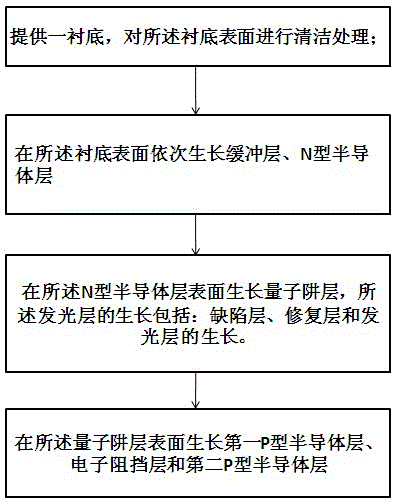
[0038] The specific implementation manner of the present invention will be described in detail below with reference to the drawings and embodiments.

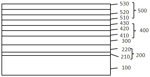
[0039] See attached figure 1 , a light-emitting diode from bottom to top: substrate 100, buffer layer 200, N-type semiconductor layer 300, quantum well layer 400, P-type semiconductor layer 500, wherein, P-type semiconductor layer 500 includes a first P-type semiconductor layer 510 , an electron blocking layer 520 and a second P-type semiconductor layer 530 ; the quantum well layer 400 is composed of a defect layer 410 , a repair layer 420 and a light emitting layer 430 . The defect layer 410 is formed by circular lamination of an InGaN well layer and a GaN barrier layer having an In / Ga content ratio C1 of 50% to 80%. The repair layer 420 is formed by cyclic lamination of InGaN well layers and GaN barrier layers with an In / Ga content ratio C2 of 45% to 60%. The thickness of each cycle of the repair layer 420 is greater than th...


PUM


Abstract

The invention discloses a light emitting diode and a preparation method of the light emitting diode. The method comprises following steps of providing a substrate; cleaning the surface of the substrate; successively growing a buffer layer and an N type semiconductor layer on the surface of the substrate; growing a quantum well layer on the surface of the N type semiconductor layer, wherein a step of growing a light emitting layer comprises growing a defect layer, a reparation layer and the light emitting layer; and growing a first P type semiconductor layer, an electron blocking layer and a second P type semiconductor layer on the quantum well layer. According to the light emitting diode and method provided by the invention, an In component is added on the premise of improving the quality of the quantum well; moreover, through adoption of the first P type layer structure of high pressure and low doping, the light emitting brightness of the light emitting diode is greatly improved.

Description

technical field [0001] The invention belongs to the technical field of semiconductor manufacturing, and in particular relates to a light emitting diode and a preparation method thereof. Background technique [0002] In recent years, the research on InGaN / GaN multi-quantum well layer as the active region of blue-green light-emitting diodes has become more and more extensive and in-depth. In the traditional LED epitaxial structure, it usually includes a buffer layer, an N-type layer, a stress release layer, a light-emitting layer, and a P-type layer. The stress release layer can only release the growth stress of the light-emitting layer. For the light-emitting layer The improvement effect of luminous efficiency is limited. [0003] In order to better solve the influence of the stress existing between the N-type layer and the light-emitting layer on the luminous efficiency of the LED device and other aspects of performance, in the prior art, the luminous efficiency of the LED ...

Claims


Application Information

Patent Timeline
Patent Type & Authority Applications(China)
IPC IPC(8): H01L33/00H01L33/02H01L33/06H01L33/32
CPCH01L33/00H01L33/06H01L33/32H01L33/0075H01L33/025H01L33/325
Inventor 林忠宝程虎林兓兓张家宏
Owner ANHUI SANAN OPTOELECTRONICS CO LTD
Why Eureka
Try Eureka