Process for growing P-type ZnO crystal film by real-time doping nitrogen

A p-type, crystal technology, applied in semiconductor/solid-state device manufacturing, ion implantation plating, coating, etc., can solve the problems of low nitrogen activity, unsatisfactory doping effect, low solid solubility, etc., and achieve good repeatability and stability effects

Inactive Publication Date: 2003-01-15
ZHEJIANG UNIV
View PDF0 Cites 8 Cited by
  • Summary
  • Abstract
  • Description
  • Claims
  • Application Information

AI Technical Summary

Problems solved by technology

The latter two doping effects are not ideal due to the deep acceptor energy level and low solid solubility, and both arsenic and phosphorus are toxic
The first two use highly active nitrogen doping and co-doping of gallium and nitrogen. Since the activity of nitrogen is very low and the atomic radius is larger than that of oxygen atoms, chemical vapor deposition (CVD) and molecular beam epitaxy (MBE) are used to grow technology, it is difficult to replace the position of oxygen atoms, and it is impossible to achieve real-time controllable nitrogen doping

Method used


Image

  • Process for growing P-type ZnO crystal film by real-time doping nitrogen
  • Process for growing P-type ZnO crystal film by real-time doping nitrogen

Examples


Embodiment Construction

[0014] The present invention is further described below in conjunction with specific examples.

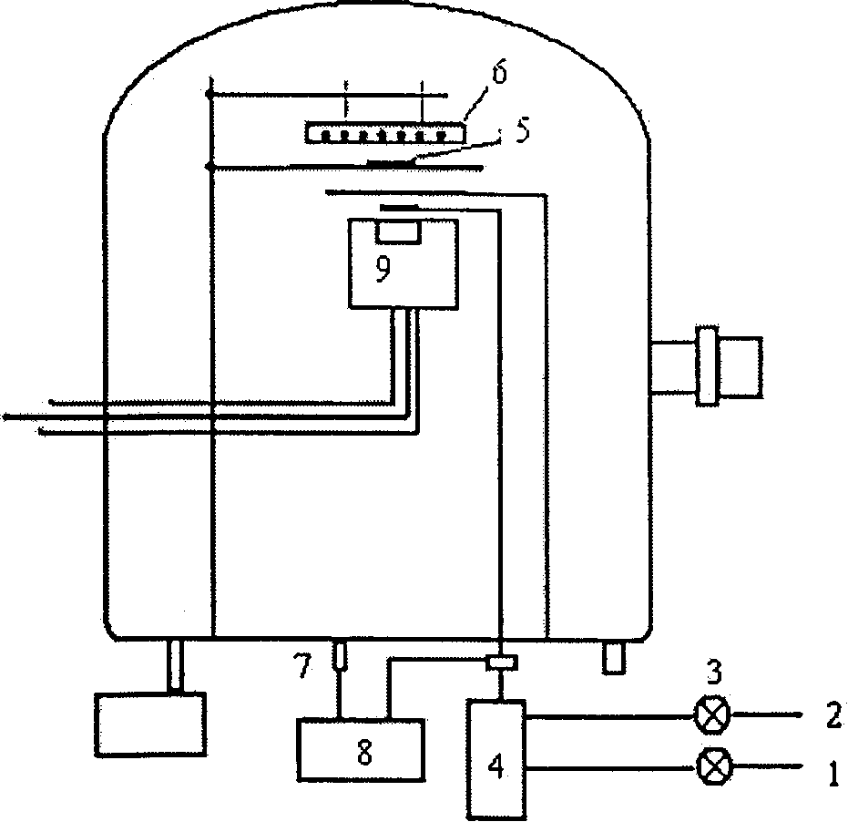
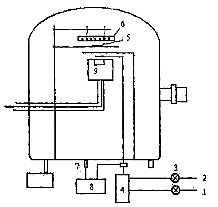
[0015] Put the substrate on the sample holder 5 of the reaction chamber after surface cleaning, and place the substrate facing down to effectively prevent the contamination of the substrate by granular impurities. The vacuum degree of the reaction chamber is pumped to 10 -3 Pa; use a heater to heat the substrate, and the substrate temperature is controlled at 500°C; the sputtering gas is high-purity NH 3 (above 99.99%) and high-purity O 2 (more than 99.99%), the two-way gas enters the buffer chamber 4 through the intake pipe 1 and 2, and is introduced into the vacuum chamber after the buffer chamber is fully mixed. The pressure in the vacuum chamber is controlled by the automatic pressure controller 8, and the pressure is about 5Pa. NH 3 with O 2 The partial pressure ratio can be adjusted arbitrarily through the flow meter 3 according to the doping requirements. In this example,...


PUM


Abstract

A process for growing P-type ZnO crystal film by real-time doping of nitrogen includes washing substrate, putting it in reaction chamber of sputter equipment, vacuumizing heating, substrate to 200-600 deg.c, introducing the mixture of high-purity NH3 and O2, and sputter growing with high-purity Zn as target under 1-10 MPa.

Description

technical field [0001] The invention relates to a doping method of p-type ZnO. Specifically, it relates to a method for growing p-type ZnO crystal thin films by doping nitrogen in real time. Background technique [0002] To realize the application of ZnO-based devices, it is necessary to prepare controllable n- and p-type ZnO crystal thin films. At present, the research on n-type ZnO crystal thin films has been relatively sufficient. By doping III-valent elements, real-time, concentration-controllable and low-resistance n-type ZnO crystal thin films can be grown. However, in order to prepare ZnO crystal thin films for optoelectronic devices, ZnO pn junctions must be prepared. Due to the existence of many intrinsic donor defects in ZnO, such as interstitial zinc Zn i and vacancy oxygen V O , and its energy levels are located at the bottom of the conduction band at 0.05eV and 0.3eV, which produces a high degree of self-compensation for the acceptor....

Claims


Application Information

Patent Timeline
IPC IPC(8): C23C14/34H01L21/20H01L21/34
Inventor 黄靖云叶志镇
Owner ZHEJIANG UNIV
Why Eureka
Try Eureka