Silicon carbide vertical field effect transistor

a technology of vertical field and transistor, which is applied in the direction of diodes, semiconductor devices, electrical apparatus, etc., can solve the problems of significant reduction of gate insulating film reliability and high voltage applied to drain electrodes, and achieve the improvement of gate insulating film reliability and gate insulating film breakdown resistan

Active Publication Date: 2014-01-09
FUJI ELECTRIC CO LTD +1
View PDF3 Cites 2 Cited by
  • Summary
  • Abstract
  • Description
  • Claims
  • Application Information

AI Technical Summary

Benefits of technology

[0018]According to the present invention, by causing an avalanche to occur under the high-concentration P-type region or in a region formed as a thin layer when high voltage is applied to the drain electrode, a large electric field is no longer applied to the gate insulating film, thereby enabling improvement in the breakdown resistance of the gate insulating film at the time of occurrence of the avalanche and enabling improvement in the reliability of the gate insulating film.

Problems solved by technology

However, if high voltage is applied to the drain electrode, particularly when the MOSFET is turned off, high voltage is applied to the drain electrode.
In this case, if a large electric field is applied to the gate insulating film, insulation breakdown of the gate insulating film may occur or the reliability of the gate insulating film may significantly be reduced.

Method used


Image

  • Silicon carbide vertical field effect transistor
  • Silicon carbide vertical field effect transistor
  • Silicon carbide vertical field effect transistor

Examples


first embodiment

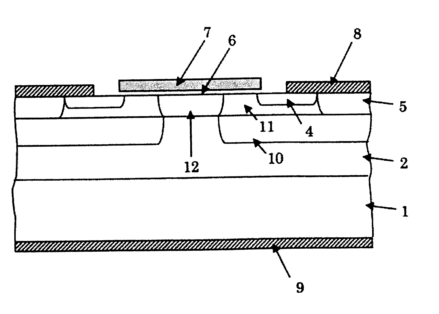
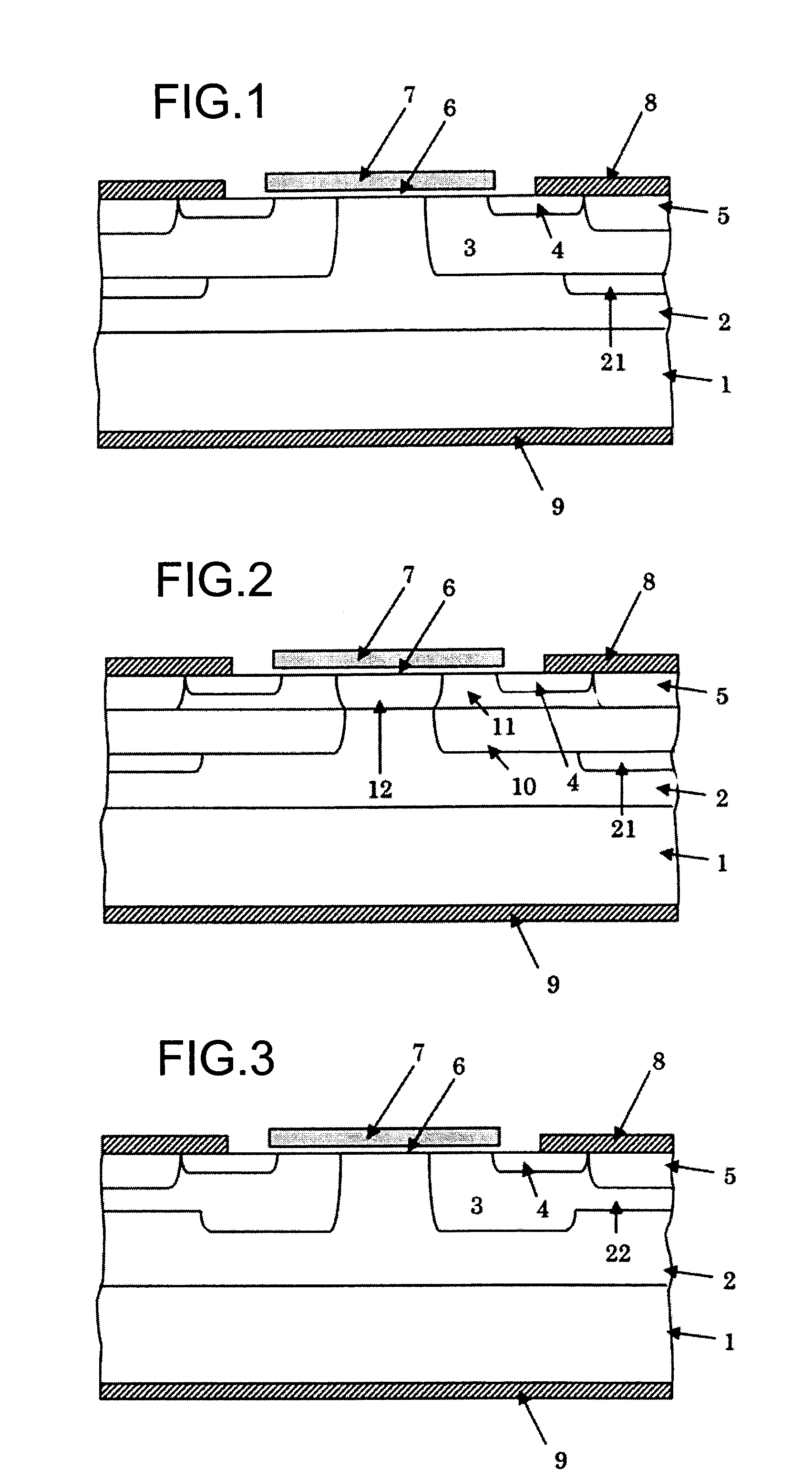
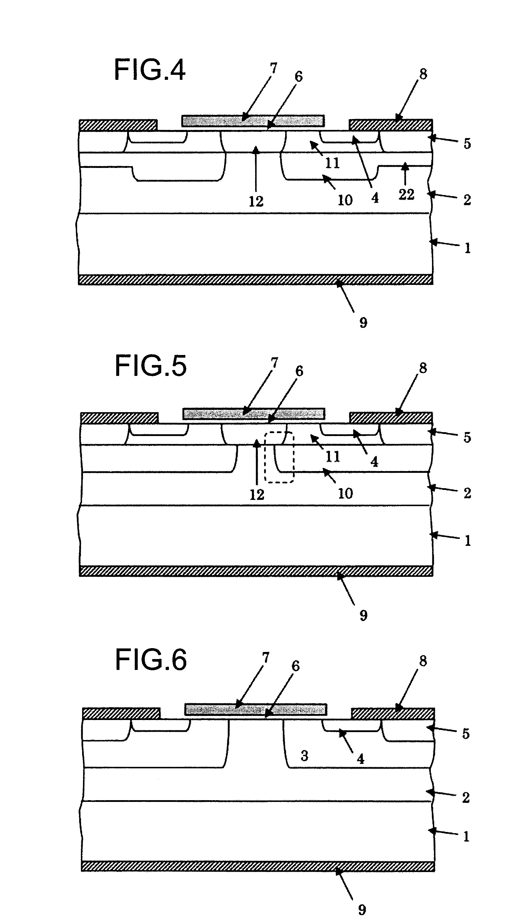
[0028]FIG. 1 depicts a cross-sectional view of a MOSFET structure according to the first embodiment of the present invention. Although a first conductive type is an N-type and a second conductive type is a P-type in the embodiments, the conductive types can be reversely formed.

[0029]In FIG. 1, an N-type SiC layer 2 is formed on a surface of an N-type SiC substrate 1 and multiple P-type regions 3 are formed on a surface of the N-type SiC layer 2.

[0030]An N-type source region 4 and a P-type contact region 5 are formed on a surface of the P-type region 3. A source electrode 8 is formed on surfaces of the N-type source region 4 and the P-type contact region 5.

[0031]A high-concentration P-type region 21 is formed under the P-type region 3. A gate electrode 7 is formed, via a gate insulting film 6, on surfaces of the P-type regions 3 and the N-type SiC layer 2 interposed between the N-type source region 4 on the surface of the P-type region 3 and an N-type source region 4 on a surface of ...

second embodiment

[0034]FIG. 2 depicts a cross-sectional view of a MOSFET according to a second embodiment of the present invention. The N-type SiC layer 2 is formed on a surface of the N-type SiC substrate 1 and multiple P-type regions 3 are formed on the surface of the N-type SiC layer 2. A P-type SiC layer 11 is further formed on the surface. An N-type region 12 is formed in the P-type SiC layer 11 to reach the N-type SiC layer 2.

[0035]The N-type source region 4 and the P-type contact region 5 are formed on a surface of the P-type SiC region 11. The source electrode 8 is formed on the surfaces of the N-type source region 4 and the P-type contact region 5.

[0036]A high-concentration P-type region 21 is formed under the P-type region 3. A gate electrode 7 is formed, via a gate insulting film 6, on surfaces of the P-type regions 3 and the N-type SiC layer 2 interposed between the N-type source region 4 on the surface of a P-type region 3 and an N-type source region 4 on a surface of another P-type reg...

third embodiment

[0038]FIG. 3 depicts a cross-sectional view of a MOSFET according to a third embodiment of the present invention.

[0039]Although the basic structure is the same as the first embodiment, a difference from the first embodiment is in that a thin P-type region 22 is formed in a portion of the P-type region 3 without forming the high-concentration P-type region 21.

[0040]The MOSFET formed in this way also causes an avalanche to occur in the PN-junction portion between the high-concentration N-type SiC layer 2 and the thin P-type region 22 when high voltage is applied to the drain electrode without a large electric field being applied to the gate oxide film, resulting in the insulation breakdown resistance and the reliability of the gate insulating film exhibiting the same characteristics as the first embodiment.


PUM


Abstract

A silicon carbide vertical field effect transistor includes a first-conductive-type silicon carbide substrate; a low-concentration first-conductive-type silicon carbide layer formed on a surface of the first-conductive-type silicon carbide substrate; second-conductive-type regions selectively formed on a surface of the first-conductive-type silicon carbide layer; first-conductive-type source regions formed in the second-conductive-type regions; a high-concentration second-conductive-type region formed between the first-conductive-type source regions in the second-conductive-type region; a source electrode electrically connected to the high-concentration second-conductive-type region and a first-conductive-type source region; a gate insulating film formed from the first-conductive-type source regions formed in adjacent second-conductive-type regions, onto the second-conductive-type regions and the first-conductive-type silicon carbide layer; a gate electrode formed on the gate insulating film; and a drain electrode on the back side of the first-conductive-type silicon carbide substrate, wherein an avalanche generating unit is disposed between the second-conductive-type region and the first-conductive-type silicon carbide layer.

Description

TECHNICAL FIELD [0001]The present invention relates to a silicon carbide vertical field effect transistor.BACKGROUND ART [0002]A silicon carbide vertical field effect transistor (see, e.g., Paten Document 1) such as a vertical MOS field effect transistor (MOSFET) is conventionally used with a semiconductor device as a switching device formed on a silicon carbide substrate. Although a silicon carbide vertical MOSFET is exemplarily illustrated and described as a silicon carbide vertical field effect transistor in this description, this is, of course, not a limitation of the present invention.[0003]FIG. 6 depicts a cross-sectional view of an N-channel MOSFET, which is a conventional silicon carbide (hereinafter abbreviated as “SiC”) field effect transistor.[0004]An N-type SiC layer 2 is formed on a surface of an N-type SiC substrate 1; multiple P-type regions 3 are formed on a surface of the N-type SiC layer 2; an N-type source region 4 and a P-type contact region 5 are formed on a sur...

Claims


Application Information

Patent Timeline
Patent Type & Authority Applications(United States)
IPC IPC(8): H01L29/06H01L29/78
CPCH01L29/0615H01L29/7827H01L29/0626H01L29/0878H01L29/1095H01L29/1608H01L29/7802H01L29/7808
Inventor HARADA, YUICHIHARADA, SHINSUKEHOSHI, YASUYUKIIWAMURO, NORIYUKI
Owner FUJI ELECTRIC CO LTD
Why Eureka
Try Eureka