Method for fabricating transistor with polymetal gate electrode

a gate electrode and polymetal technology, applied in the direction of semiconductor devices, electrical equipment, basic electric elements, etc., can solve the problems of prolonging delay time, difficult and the gate electrode with the polycide structure is still limited to overcome the required rapid operation speed of highly integrated semiconductor devices. , to achieve the effect of improving the vertical resistance of the gate electrod

Inactive Publication Date: 2006-04-18
SK HYNIX INC
View PDF11 Cites 30 Cited by
  • Summary
  • Abstract
  • Description
  • Claims
  • Application Information

AI Technical Summary

Benefits of technology

[0011]It is, therefore, an object of the present invention to provide a method for fabricating a transistor with a polymetal gate electrode structure to which a selective re-oxidation process is applied without being affected by metal contaminations.
[0012]It is another object of the present invention to provide a method for fabricating a transistor with a polymetal gate electrode structure capable of improving a vertical resistance of the gate electrode by suppressing or blocking oxidation of an interfacial surface between a metal layer and a polysilicon layer during the gate re-oxidation process.
[0013]In accordance with an aspect of the present invention, there is provided a method for fabricating a transistor with a polymetal gate electrode structure, including the steps of: forming a gate insulation layer on a substrate; forming a patterned gate stack structure on the gate insulation layer, wherein the patterned stack structure includes a polysilicon layer as a bottom layer and a metal layer as an upper layer; forming a silicon oxide-based capping layer along a profile containing the patterned gate stack structure and on the gate insulation layer at a predetermined temperature that prevents oxidation of the metal layer; and performing a gate re-oxidation process.
[0014]In accordance with another aspect of the present invention, there is also provided a method for fabricating a semiconductor device with a polymetal gate electrode structure, including the steps of: forming a gate oxide layer on a substrate; forming a gate stack structure by sequentially stacking and subsequently etching a polysilicon layer, a diffusion barrier layer, a tungsten layer and a hard mask insulation layer on the gate oxide layer; forming a silicon oxide layer on a surface of the gate oxide layer exposed by the etching and along a profile containing the gate stack structure by performing an ALD technique at a predetermined temperature that prevents oxidation of the metal layer; and performing a gate re-oxidation process.

Problems solved by technology

However, it is difficult to apply polysilicon used for the typical gate electrode into a device requiring a rapid operation speed due to high resistivity of the polysilicon, which is a cause for prolonging delay time.
This difficulty is pronounced as a device becomes more highly integrated.
However, the gate electrode with the polycide structure is still limited to overcome the required rapid operation speed of a highly integrated semiconductor device.
Despite of these advantages of the re-oxidation process, there is a problem of an abrupt expansion of volume because tungsten is oxidized during the re-oxidation process.
However, the selective re-oxidation process may have several problems.
This gaseous contaminant WH2O4 may contaminate a wafer and a chamber, impairing subsequent processes and deteriorating device characteristics.
In addition to tungsten (W), such metal as molybdenum (Mo), titanium (Ti), tantalum (Ta), ruthenium (Ru), iridium (Ir) and platinum (Pt) used for the polymetal gate electrode structure may have the same problem of contamination.
This formation of the insulation layer may increase a vertical resistance of the gate electrode, thereby delaying a signal during a high-frequency operation.

Method used


Image

  • Method for fabricating transistor with polymetal gate electrode
  • Method for fabricating transistor with polymetal gate electrode
  • Method for fabricating transistor with polymetal gate electrode

Examples


Embodiment Construction

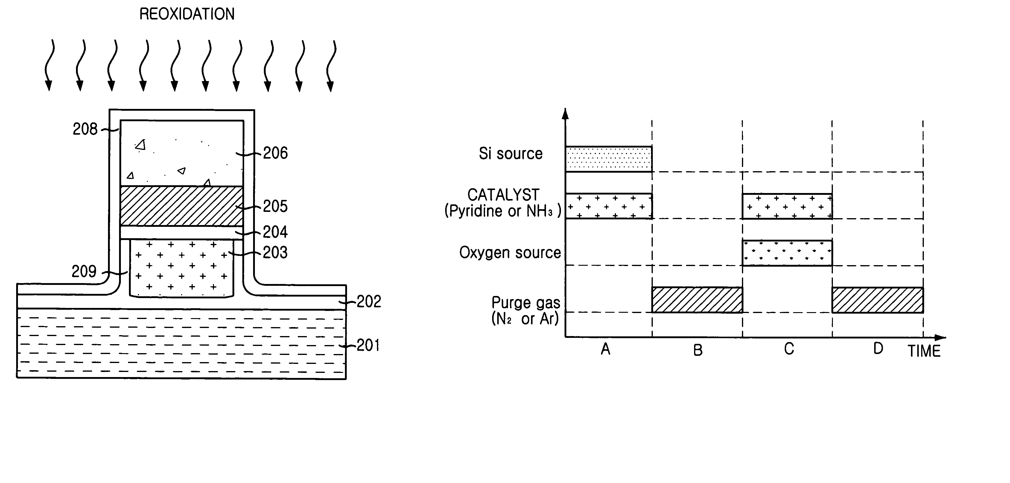
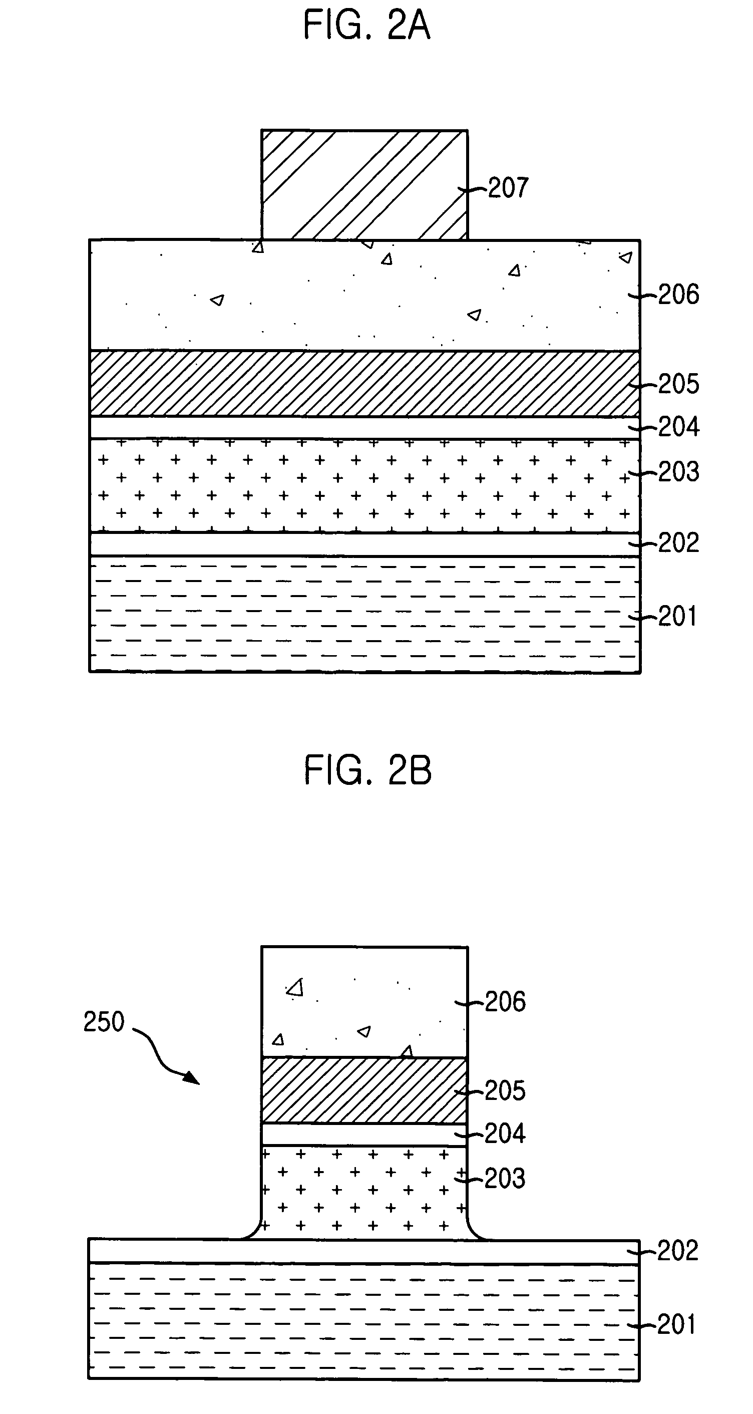
[0022]Hereinafter, detailed descriptions on a method for fabricating a metal-oxide semiconductor (MOS) transistor with a polymetal gate electrode structure will be provided in the following with reference to the accompanying drawings.

[0023]FIGS. 2A to 2D are cross-sectional views of a MOS transistor with a polymetal gate electrode structure containing stacked layers of tungsten, tungsten nitride and polysilicon (W / WNx / Poly-Si) in accordance with a preferred embodiment of the present invention.

[0024]Referring to FIG. 2A, a gate oxide layer 202, a polysilicon layer 203, a tungsten nitride (WNx) layer 204, a tungsten (W) layer 205 and a hard mask insulation layer 206 are sequentially formed on a substrate 201 through a deposition and / or growth process. A photoresist pattern 207 for patterning a gate electrode is formed on this stack structure. Herein, the tungsten nitride layer 204 is a diffusion barrier layer.

[0025]Referring to FIG. 2B, the hard mask insulation layer 206, the tungsten...


PUM


Abstract

The present invention is related to a method for fabricating a transistor with a polymetal gate electrode structure. The method includes the steps of: forming a gate insulation layer on a substrate; forming a patterned gate stack structure on the gate insulation layer, wherein the patterned stack structure includes a polysilicon layer as a bottom layer and a metal layer as an upper layer; forming a silicon oxide-based capping layer along a profile containing the patterned gate stack structure and on the gate insulation layer at a predetermined temperature that prevents oxidation of the metal layer; and performing a gate re-oxidation process.

Description

FIELD OF THE INVENTION[0001]The present invention relates to a method for fabricating a transistor with a polymetal gate electrode; and, more particularly, to a method for fabricating a transistor with a polymetal gate electrode through the use of a re-oxidation process free from metal contamination and capable of improving a vertical resistance by suppressing interfacial oxidation of the polymetal.DESCRIPTION OF RELATED ARTS[0002]Generally, a gate electrode of a metal-oxide semiconductor (MOS) transistor is made of polysilicon. Also, large-scale of integration contributes to micronization of various patterns including a gate electrode. However, it is difficult to apply polysilicon used for the typical gate electrode into a device requiring a rapid operation speed due to high resistivity of the polysilicon, which is a cause for prolonging delay time.[0003]This difficulty is pronounced as a device becomes more highly integrated. Thus, a gate electrode with a polycide structure is for...

Claims


Application Information

Patent Timeline
Patent Type & Authority Patents(United States)
IPC IPC(8): H01L21/4763H01L21/44H01L21/336H01L21/28H01L21/3205
CPCH01L21/28247H01L21/28061H01L21/18
Inventor LIM, KWAN-YONGHONG, BYUNG-SEOPCHO, HEUNG-JAELEE, JUNG-HOOH, JAE-GEUNKIM, YONG-SOOJANG, SE-AUGYANG, HONG-SEONSOHN, HYUN-CHUL
Owner SK HYNIX INC
Why Eureka
Try Eureka