Glass ceramic substrate and method for producing the same

a technology of glass ceramic and substrate, which is applied in the direction of fixed capacitor details, fixed capacitors, coatings, etc., can solve the problems of reducing the conductivity of the surface electrode on its surface, reducing the conductivity of the surface electrode, and making the plating layer more likely to peel off, so as to improve the coplanarity of the glass ceramic substrate and reduce the amount of glass. , the effect of reliable reduction of glass

Active Publication Date: 2014-01-23
MURATA MFG CO LTD
View PDF17 Cites 7 Cited by
  • Summary
  • Abstract
  • Description
  • Claims
  • Application Information

AI Technical Summary

Benefits of technology

[0013]An object of the present invention is therefore to provide a glass ceramic substrate with improved peeling resistance in the interface between a surface electrode and a glass ceramic layer and between a plating layer and the surface electrode, and a method for producing such a glass ceramic substrate.
[0019]In these aspects of the invention, the use of Al2O3 as the non-vitreous inorganic oxide is advantageous.
[0020]These aspects of the invention achieve a situation where the abundance ratio of non-vitreous inorganic oxide in the surface electrode is lower in the region bordering the plating layer than in the region bordering the glass ceramic layer at least in the edge portion in a plan view. This reduces the amount of glass that gets exposed on the surface of the surface electrode, thereby ensuring good conductivity and, therefore, good platability, making the plating layer more firmly adhere to the surface electrode and less likely to peel off of the surface electrode.
[0022]This method for producing a glass ceramic substrate according to the second aspect of the invention becomes more reliable in reducing the amount of glass that gets exposed on the surface of the surface electrode when the second conductive paste contains no non-vitreous inorganic oxide.
[0023]Furthermore, the surface electrode becomes less likely to peel off of the glass ceramic layer when the first conductive paste contains 7% or more by volume the non-vitreous inorganic oxide based on the total volume thereof.
[0024]Moreover, the coplanarity of the glass ceramic substrate is improved when the second paste film covers only the edge portion of the first paste film in a plan view like a picture frame.

Problems solved by technology

In both cases, insufficient bonding of the surface electrode to the glass ceramic layer causes the electrode to peel off.
In general, a surface electrode formed by a printing process (e.g., screen printing) using a conductive paste tends to be thinner in the edge portion in a plan view than in the middle portion because of the effects of printing defects such as running and bleeding of the printed paste.
Thus, the use of the conductive paste described in Patent Document 1 to form a surface electrode may result in reduced conductivity of the surface electrode on its surface because the glass component drawn up from the ceramic layer into the surface electrode is likely to reach the surface of the electrode and get exposed particularly in the edge portion in a plan view, the portion where the surface electrode is relatively thin.
If the glass component is exposed on the surface of the surface electrode as described above, however, reduced platability of the surface electrode makes the plating layer more likely to peel off of it.
In particular, reduced platability of the surface electrode in the edge portion in a plan view leads to a significantly low peeling resistance.Patent Document 1: Japanese Unexamined Patent Application Publication No. 2000-173346

Method used


Image

  • Glass ceramic substrate and method for producing the same
  • Glass ceramic substrate and method for producing the same
  • Glass ceramic substrate and method for producing the same

Examples


embodiment 1

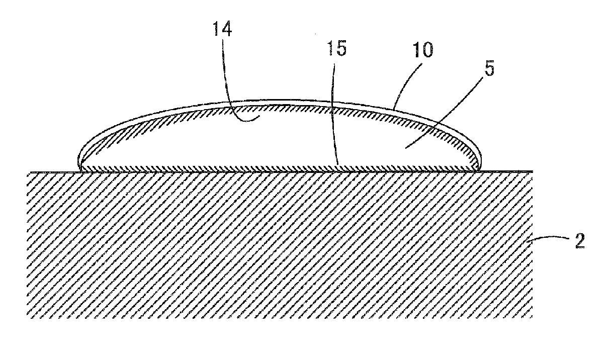
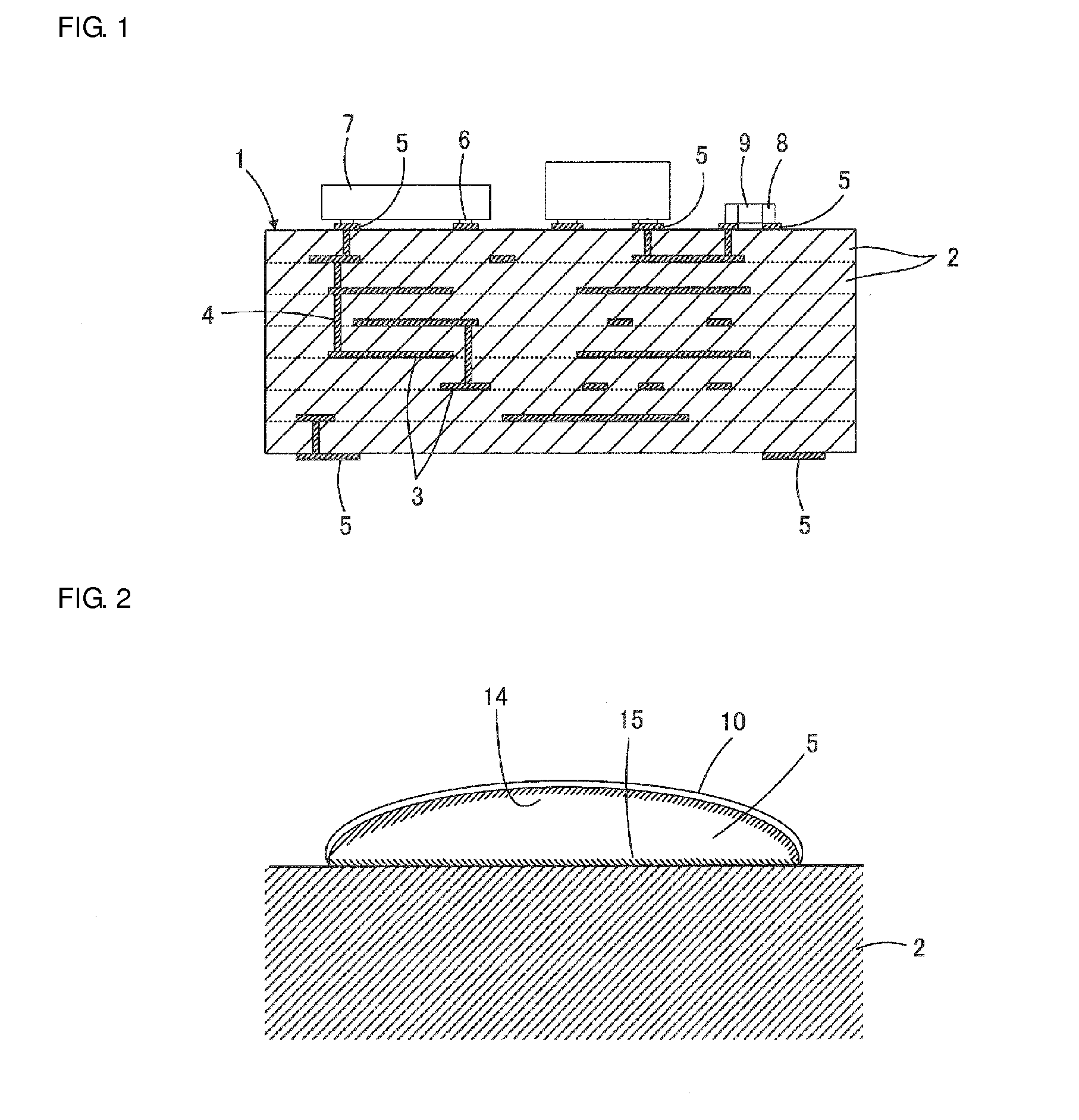
[0031]The following describes a glass ceramic substrate 1 of the invention with reference to FIG. 1.

[0032]The glass ceramic substrate 1 is a multilayer ceramic substrate and has a laminated structure containing a stack of several glass ceramic layers 2. The glass ceramic substrate 1 contains various wiring conductors, including those that form passive elements such as capacitors and inductors, and those used to establish connections such as electrical connections between elements. Some of the wiring conductors are placed in the glass ceramic substrate 1, and some others are on the outer surface.

[0033]Examples of the wiring conductors placed in the glass ceramic substrate 1 include internal electrodes 3, which are formed along the interfaces between the glass ceramic layers 2, and via-hole conductors 4, which are formed through the glass ceramic layers 2 to provide interlayer connections.

[0034]Surface electrodes 5 are wiring conductors formed on the surface of the glass ceramic subs...

embodiment 2

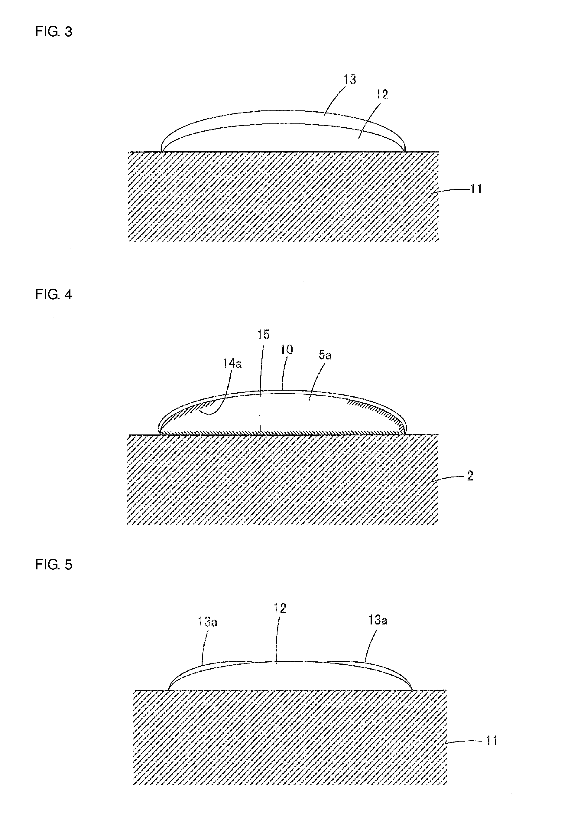
[0048]The following describes Embodiment 2 of the invention with reference to FIGS. 4 and 5. FIGS. 4 and 5 correspond to FIGS. 2 and 3, respectively. In FIGS. 4 and 5, like reference signs represent like elements in FIGS. 2 and 3. The details of the elements already described herein are omitted in the following.

[0049]A characteristic of Embodiment 2 is that the second paste film 13a covers only the edge portion of the first paste film 12 in a plan view like a picture frame as illustrated in FIG. 5. The configuration of the first paste film 12 and the second paste film 13a in a plan view is as in FIG. 6 (C), which is described later herein.

[0050]In Embodiment 2, in which the second paste film 13a is formed like a picture frame, the abundance ratio of non-vitreous inorganic oxide is relatively low in the edge portion of the surface electrode 5a in a plan view, i.e., the region derived from the second paste film 13a. As a result, the abundance ratio of non-vitreous inorganic oxide in t...


PUM

PropertyMeasurementUnit
particle diameteraaaaaaaaaa
thicknessaaaaaaaaaa
thicknessaaaaaaaaaa

Abstract

A first paste film containing a metal powder and non-vitreous inorganic oxide is formed on a glass ceramic green sheet, and a second paste film containing a metal powder is formed on the first paste film to cover at least the edge portion of the first paste film. Then the glass ceramic green sheet and the first and second paste films are fired. As a result, a surface electrode is obtained, and then a plating layer is formed on the surface electrode. The second paste film contains less non-vitreous inorganic oxide than the first paste film and the abundance ratio of the non-vitreous inorganic oxide in the surface electrode is lower in a region bordering the plating layer than in a region bordering the glass ceramic layer at least in an edge portion of the surface electrode.

Description

CROSS REFERENCE TO RELATED APPLICATIONS[0001]The present application is a continuation of International application No. PCT / JP2012 / 055373, filed Mar. 2, 2012, which claims priority to Japanese Patent Application No. 2011-069411, filed Mar. 28, 2011, the entire contents of each of which are incorporated herein by reference.FIELD OF THE INVENTION[0002]The present invention relates to a glass ceramic substrate and a method for producing a glass ceramic substrate and, in particular, to a glass ceramic substrate having a surface electrode and a method for producing such a glass ceramic substrate.BACKGROUND OF THE INVENTION[0003]An example of a known glass ceramic substrate is a laminated, multilayer ceramic substrate, which contains a stack of glass ceramic layers. A laminated glass ceramic substrate contains various wiring conductors, including those that form passive elements such as capacitors and inductors, and those used to establish connections such as electrical connections betwee...

Claims


Application Information

Patent Timeline
Patent Type & Authority Applications(United States)
IPC IPC(8): H01G4/10
CPCH01G4/105H05K1/111H05K3/4629H05K3/246H05K3/4007H05K2201/035H05K2203/1476
Inventor WAKAKI, SUMIYOSUMI, TAKAHIROMOTOYA, MACHIKO
Owner MURATA MFG CO LTD
Why Eureka
Try Eureka