Sealing Structure and Organic Electroluminescence Device

a technology of electroluminescence device and sealing structure, which is applied in the direction of thermoelectric devices, transportation and packaging, and other domestic objects, can solve the problems of glass frit not being melted sufficiently, performance degrades rapidly, and differences in temperature distribution, so as to achieve high air tightness and high air tightness , the flexibility of the layout of the first metal layer serving as a common power supply line can be increased

Active Publication Date: 2014-01-30
SEMICON ENERGY LAB CO LTD
View PDF8 Cites 35 Cited by
  • Summary
  • Abstract
  • Description
  • Claims
  • Application Information

AI Technical Summary

Benefits of technology

[0018]With the structures of a sealing structure and an organic electroluminescence device of one embodiment of the present invention, a sealing structure with high air-tightness and an or

Problems solved by technology

It is known that when the organic electroluminescence element is exposed to the air (including moisture, oxygen, and the like), its performance degrades rapidly.
Therefore, in the case where the degree of overlap between the common power supply lines and the glass frit varies depending on the loca

Method used


Image

  • Sealing Structure and Organic Electroluminescence Device
  • Sealing Structure and Organic Electroluminescence Device
  • Sealing Structure and Organic Electroluminescence Device

Examples


embodiment 1

[0028]A structure of a sealing structure which is one embodiment of the present invention is described below in detail.

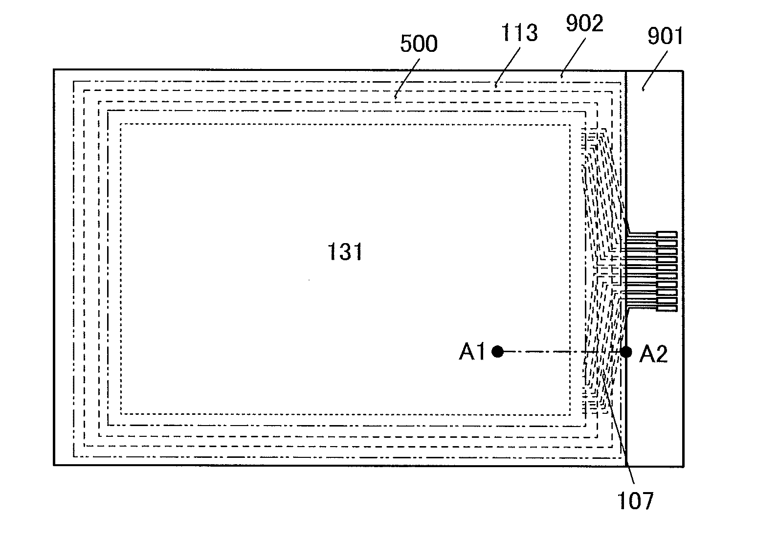
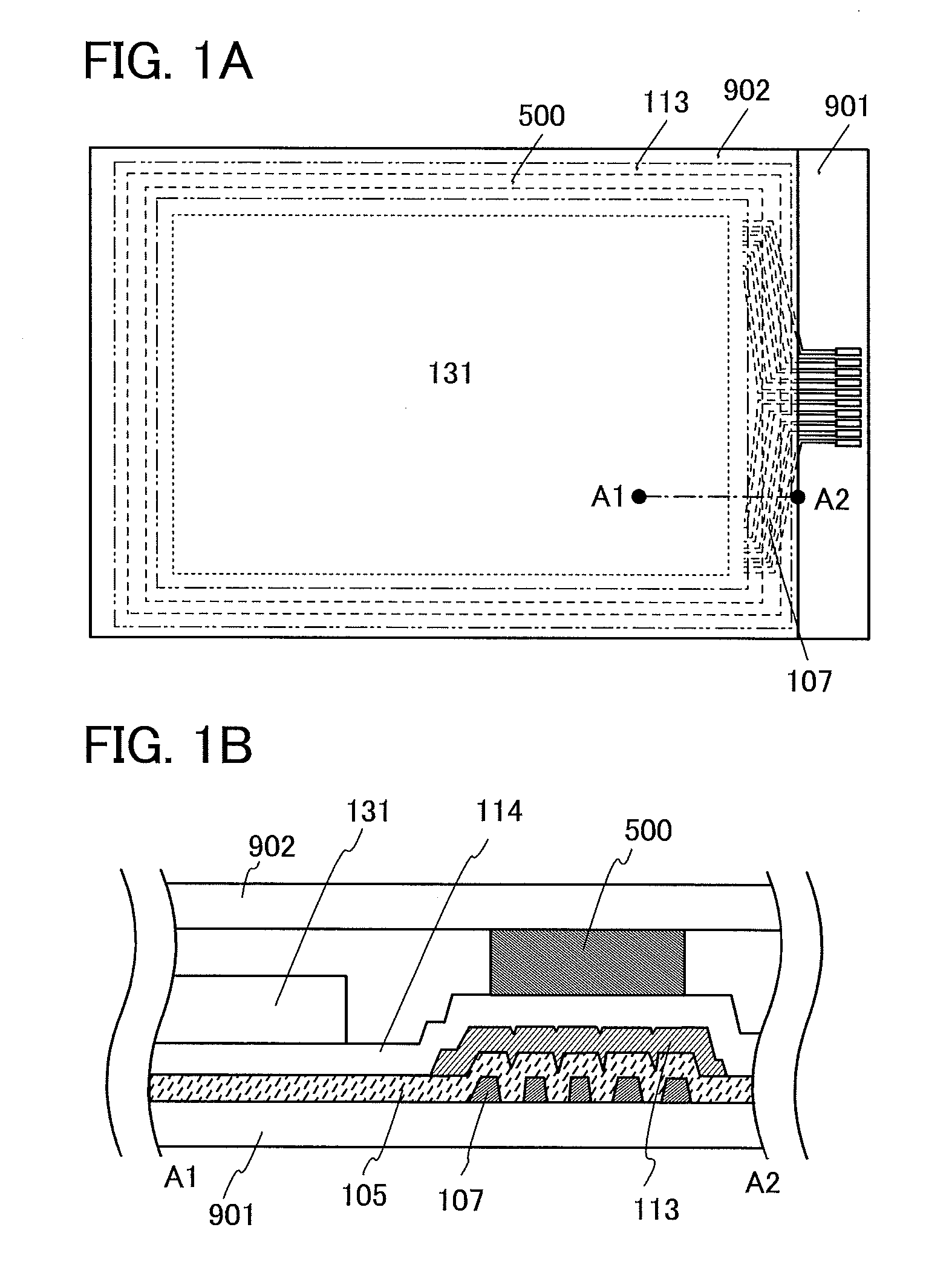
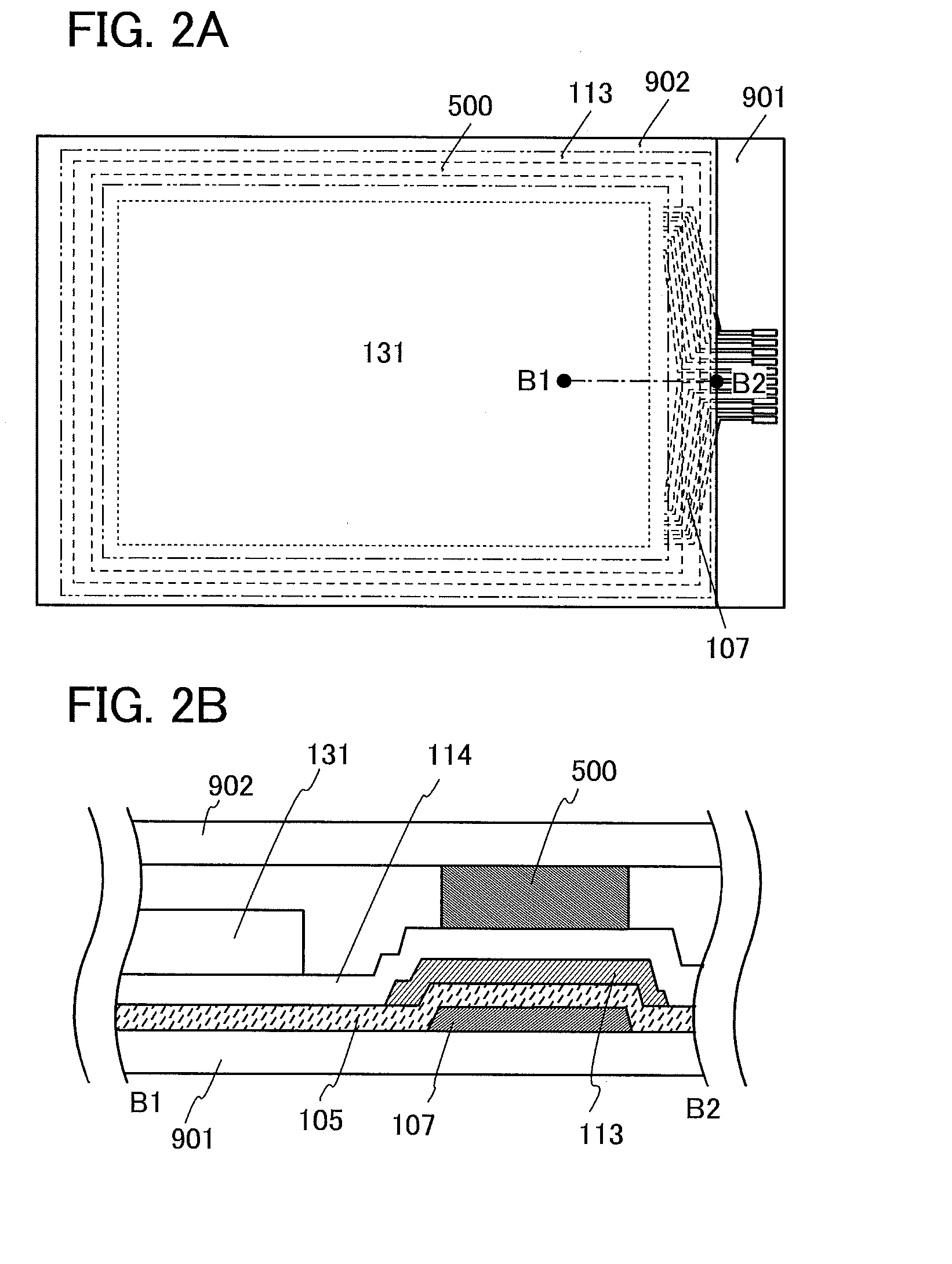
[0029]FIG. 1A and FIG. 2A are top views of a sealing structure, and FIG. 1B and FIG. 2B are schematic cross-sectional views of part of the sealing structure.

[0030]In the sealing structure illustrated in FIG. 1B, a light-emitting element 131 is sealed by a first substrate 901, a second substrate 902, and a sealant 500. A first metal layer 107 is provided over the first substrate 901 and a first insulating layer 105 is provided in contact with the first metal layer 107. A second metal layer 113 is provided so as to overlap with the sealant 500 and be in contact with the first insulating layer 105. A second insulating layer 114 is provided in contact with the first insulating layer 105 and the sealant 500. The first metal layer 107 is covered with the second metal layer 113 with the first insulating layer 105 therebetween, and the second metal layer 113 is provided bet...

modification example

[0040]FIG. 8 illustrates a modification example of the sealing structure of FIG. 2B and the second metal layer 113 is provided with holes. The second insulating layer 114 provided in contact with the second metal layer 113 has an uneven surface due to the holes. The sealant 500 fills in the unevenness provided in the second insulating layer 114; thus, an anchor effect is caused. Therefore, the adhesion between the sealant 500 and the second insulating layer 114 is increased and a sealing structure with high air-tightness can be obtained.

[0041]This embodiment can be combined with any of the other embodiments disclosed in this specification as appropriate.

embodiment 2

[0042]A structure of an organic electroluminescence device which is one embodiment of the present invention is described below in detail.

[0043]FIG. 3A and FIG. 4A are top views of an organic electroluminescence device, and FIG. 3B and FIG. 4B are schematic cross-sectional views of part of the organic electroluminescence device, in which specific structures of a sealing portion 4501, a pixel portion 4502, and a signal line circuit portion 4503 are shown.

[0044]As illustrated in FIG. 3B, the organic electroluminescence device includes the first substrate 901, a buffer layer 103, a plurality of transistors, the second insulating layer 114, a planarization layer 116, a light-emitting element 130, partition walls 124, and the second substrate 902 in the pixel portion 4502.

[0045]As illustrated in FIG. 3B, the plurality of transistors is provided over the first substrate 901, and the light-emitting element 130 is provided over each of transistors 150 and 151. Each transistor includes a gate...


PUM

PropertyMeasurementUnit
Melting pointaaaaaaaaaa
aaaaaaaaaa

Abstract

A sealing structure with high air-tightness and an organic electroluminescence device with high air-tightness are provided regardless of a pattern of a first metal layer overlapping with glass frit. A second metal layer is provided in a region where a common power supply line overlaps with the glass frit. Since laser light is absorbed or reflected by the second metal layer, the glass frit can be uniformly heated. Therefore, an object to be sealed can be sealed with a low-melting-point glass in which a crack is not easily generated.

Description

BACKGROUND OF THE INVENTION[0001]1. Field of the Invention[0002]The present invention relates to a sealing structure and an organic electroluminescence device.[0003]2. Description of the Related Art[0004]Research and development have been extensively conducted on organic electroluminescence elements. In the fundamental structure of the organic electroluminescence element, a layer containing a light-emitting organic compound is interposed between a pair of electrodes. By applying voltage to this element, light emission from the light-emitting organic compound can be obtained.[0005]The light-emitting device using an organic electroluminescence element is, for example, a lighting device, or an image display device including a thin film transistor. The organic electroluminescence element can be formed in a film shape and thus easily increased in area, which allows a lighting device with a planar light source to be realized. In addition, an image display device using an organic electrolu...

Claims


Application Information

Patent Timeline
IPC IPC(8): H01L51/52B32B7/14H05B44/00
CPCB32B7/14H01L51/5253B32B7/12B32B9/002B32B9/005B32B15/043B32B15/18B32B15/20B32B3/30B32B2255/06B32B2255/26B32B2307/206B32B2457/00Y10T428/239H10K59/131H10K50/8426H05B33/04H10K50/844
Inventor NISHIDO, YUSUKE
Owner SEMICON ENERGY LAB CO LTD
Why Eureka
Try Eureka