Fluctuation Resistant Low Access Resistance Fully Depleted SOI Transistor with Improved Channel Thickness Control and Reduced Access Resistance

a technology of soi transistor and fluctuation resistance, which is applied in the manufacture of metaloxidesemiconductor field effect transistors, and can solve the problems of long-standing troublesome mos transistors, step changes in drain current, and un-depleted doped transistors

Active Publication Date: 2014-01-30
SEMIWISE
View PDF2 Cites 9 Cited by
  • Summary
  • Abstract
  • Description
  • Claims
  • Application Information

AI Technical Summary

Problems solved by technology

MOS transistors have long been troubled by the adverse effects of their underlying substrates, like parasitic capacitance and area-consuming isolation.
The un-depleted doped region beneath the gate of a PD SOI transistor proved to have its own disadvantages, largely caused by its tendency to charge and discharge resulting in step changes in the drain current.
These deviations are devastating when billions of transistors are integrated into a single integrated circuit chip.
Layers in the sub-10 nm thickness range present manufacturing challenges, and the very thin layers have an adverse effect on performance because the parasitic series resistance in sources and drains cuts down on the transistors' gain figures.
Further, the prior art structure remains subject to variations associated with the randomness of the drain-channel interface, and its source and drain conductances are limited by the very thin film thickness.

Method used


Image

  • Fluctuation Resistant Low Access Resistance Fully Depleted SOI Transistor with Improved Channel Thickness Control and Reduced Access Resistance
  • Fluctuation Resistant Low Access Resistance Fully Depleted SOI Transistor with Improved Channel Thickness Control and Reduced Access Resistance
  • Fluctuation Resistant Low Access Resistance Fully Depleted SOI Transistor with Improved Channel Thickness Control and Reduced Access Resistance

Examples


Embodiment Construction

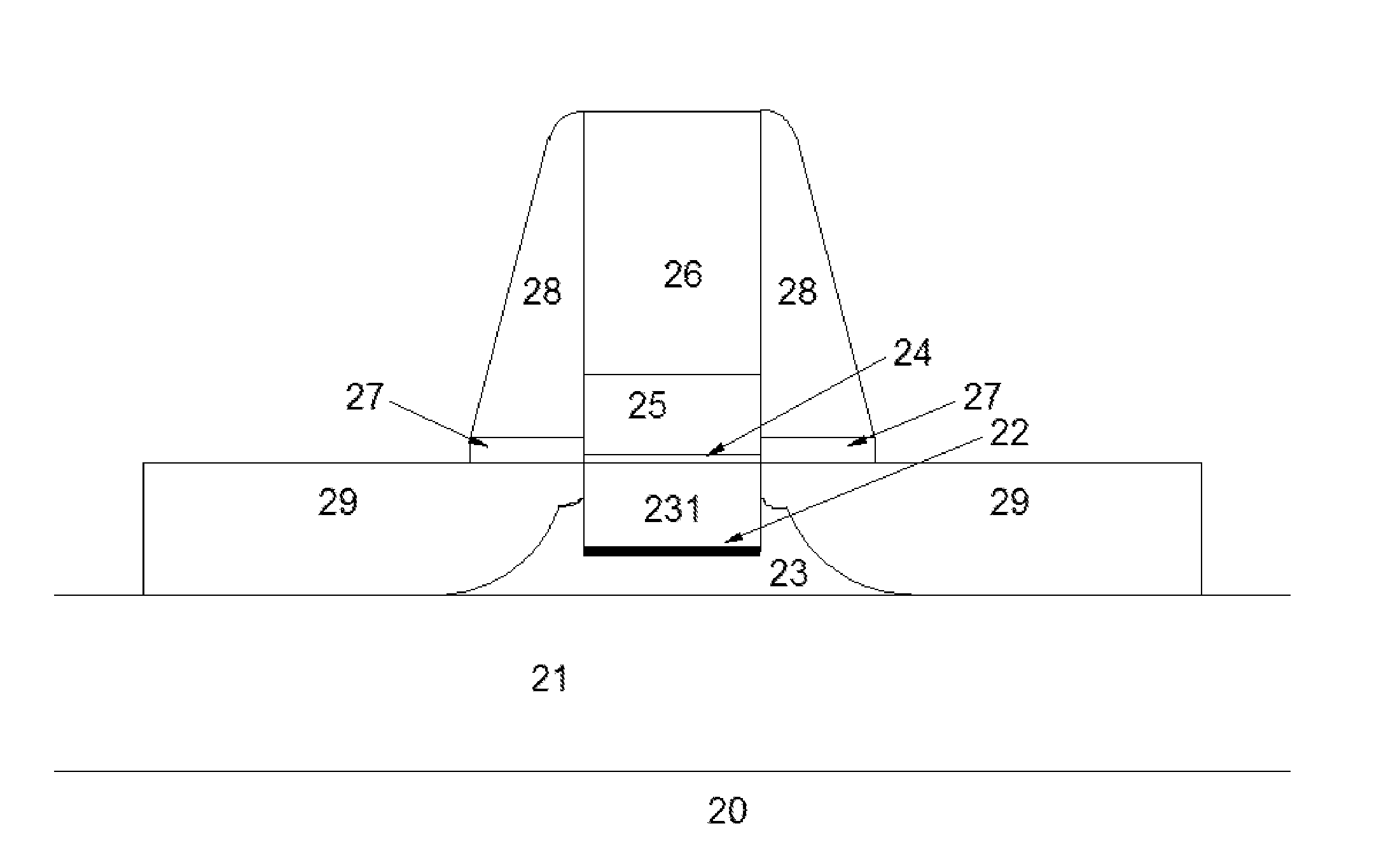
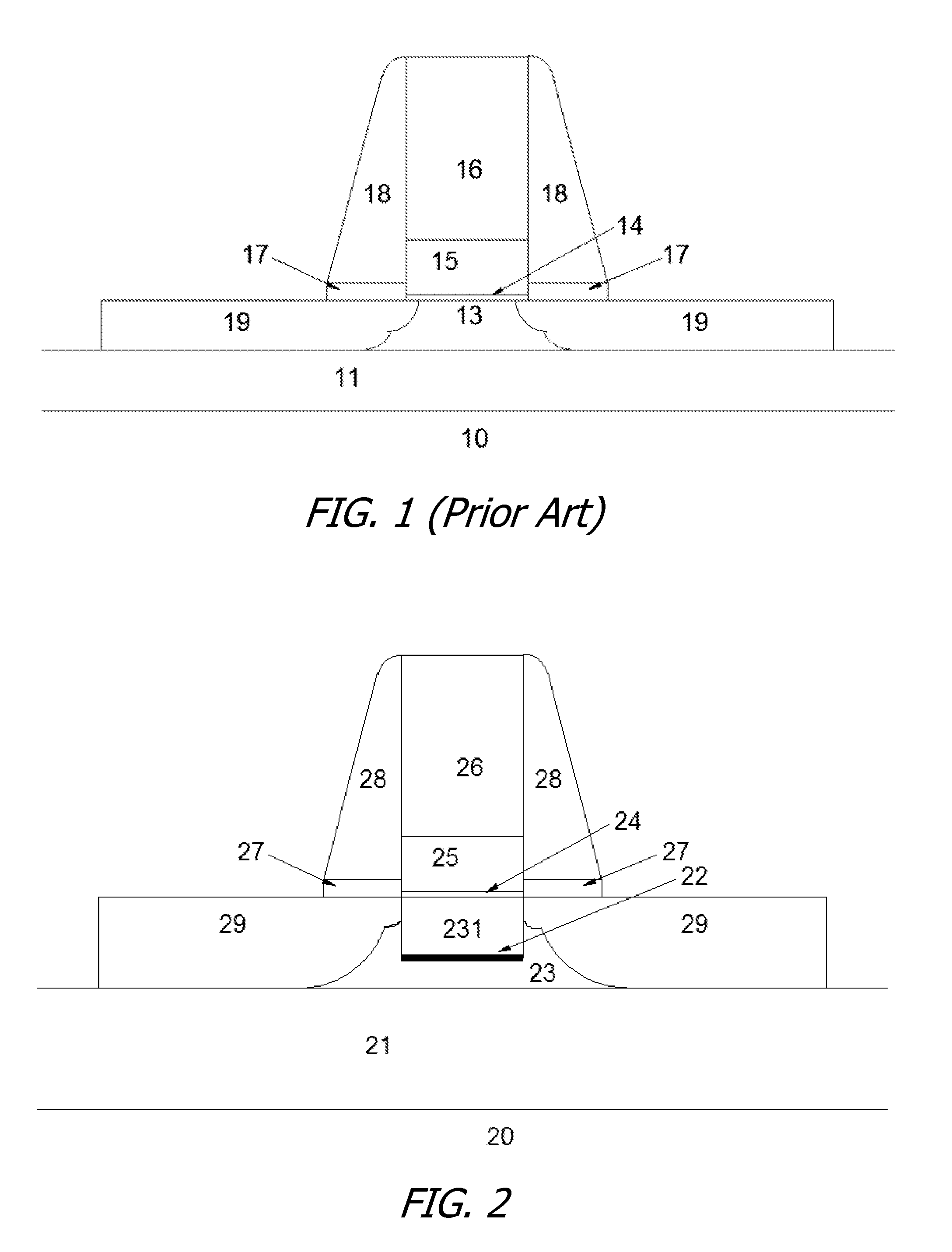
[0016]The structure, and fabrication method thereof, implements a fully depleted silicon-on-insulator (SOI) transistor using a “Channel Last” procedure in which the active channel is a low-temperature epitaxial layer in an etched recess in the SOI silicon film. An optional δ-layer of extremely high doping allows its threshold voltage to be set to a desired value. Based on high-K metal gate last technology, this transistor has reduced threshold uncertainty and superior source and drain conductance. The use of epitaxial layer improves the thickness control of the active channel and reduces the process induced variations. The utilization of active silicon layer that is two or more times thicker than those used in conventional fully depleted SOI devices, reduces the access resistance and improves the on-current of the SOI transistor.

[0017]Embodiments of the invention achieve extremely low random variability in fully depleted SOI transistors by modifying the transistor structure to subst...


PUM


Abstract

The structure, and fabrication method thereof, implements a fully depleted silicon-on-insulator (SOI) transistor using a “Channel Last” procedure in which the active channel is a low-temperature epitaxial layer in an etched recess in the SOI silicon film. An optional δ-layer of extremely high doping allows its threshold voltage to be set to a desired value. Based on high-K metal gate last technology, this transistor has reduced threshold uncertainty and superior source and drain conductance. The use of epitaxial layer improves the thickness control of the active channel and reduces the process induced variations. The utilization of active silicon layer that is two or more times thicker than those used in conventional fully depleted SOI devices, reduces the access resistance and improves the on-current of the SOI transistor.

Description

CROSS-REFERENCE TO RELATED APPLICATIONS[0001]This application claims the benefit of U.S. Provisional Patent Application No. 61 / 676,932 filed Jul. 28, 2012.BACKGROUND OF THE INVENTION[0002]1. Field of the Invention[0003]The invention generally relates to the manufacturing of metal-oxide-semiconductor field effect transistors (MOSFETs), and more particularly to transistors fabricated in thin silicon films over an insulating layer, usually referred to as “buried oxide” or BOX. Even more specifically, this invention deals with those instances where random variations of the threshold voltages of MOSFETs adversely affect integrated circuit yield and performance.[0004]2. Prior Art[0005]MOS transistors have long been troubled by the adverse effects of their underlying substrates, like parasitic capacitance and area-consuming isolation. In the earliest days of integrated circuit (IC) technology, the use of a thin film of silicon on a sapphire substrate was proposed as a solution to these pro...

Claims


Application Information

Patent Timeline
Patent Type & Authority Applications(United States)
IPC IPC(8): H01L29/78H01L29/66
CPCH01L29/66477H01L29/78H01L29/4983H01L29/1041H01L29/66545H01L29/66621H01L29/66651H01L29/7833
Inventor ASENOV, ASEN
Owner SEMIWISE
Why Eureka
Try Eureka