Through-holed interposer, packaging substrate, and methods of fabricating the same

Active Publication Date: 2014-01-30
UNIMICRON TECH CORP
View PDF7 Cites 19 Cited by
  • Summary
  • Abstract
  • Description
  • Claims
  • Application Information

AI Technical Summary

Benefits of technology

[0009]In view of the above-mentioned problems of the prior art, an interposer is disposed between a packaging substrate and a semiconductor additionally. The interposer has through-silicon vias (TSVs) and a redistribution layer (RDL) formed on the TSVs. One end of each of the TSV is connectable to a

Problems solved by technology

However, the low-k dielectric material is porous and fragile.
Although the semiconductor chip 12 having a high dens

Method used


Image

  • Through-holed interposer, packaging substrate, and methods of fabricating the same
  • Through-holed interposer, packaging substrate, and methods of fabricating the same
  • Through-holed interposer, packaging substrate, and methods of fabricating the same

Examples


Embodiment Construction

[0020]The following illustrative embodiments are provided to illustrate the disclosure of the present invention, these and other advantages and effects can be apparently understood by those in the art after reading the disclosure of this specification. The present invention can also be performed or applied by other different embodiments. The details of the specification may be on the basis of different points and applications, and numerous modifications and variations can be devised without departing from the spirit of the present invention.

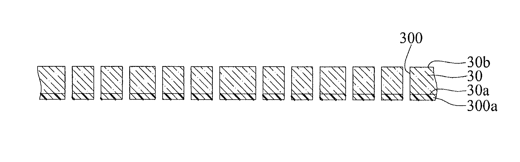
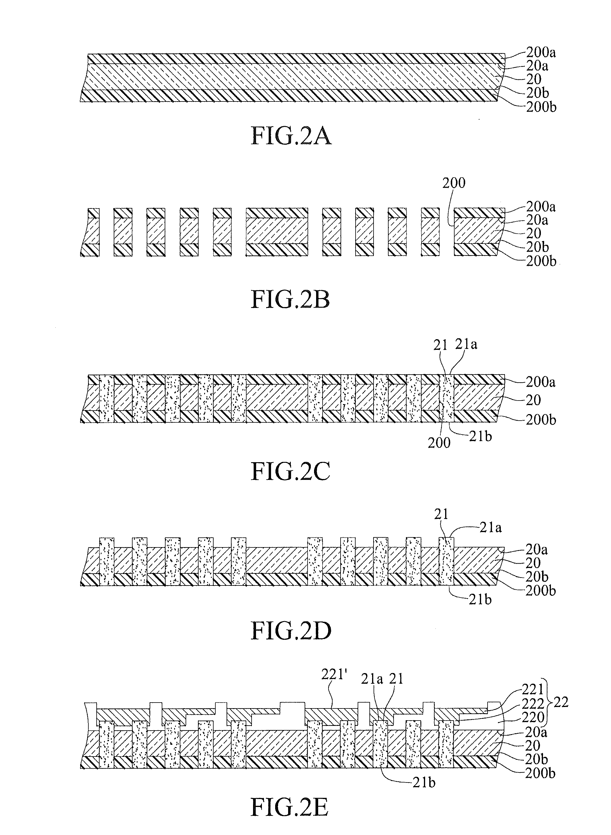
[0021]FIGS. 2A to 2H are cross-sectional views illustrating a method of fabricating a through-holed interposer 2 according to the present invention.

[0022]As shown in FIG. 2A, a board body 20 has opposing first surface 20a and second surface 20b, and a first protection layer 200a and a second protection layer 200b are formed on the first surface 20a and the second surface 20b, respectively.

[0023]In an embodiment, the board body 20 is made of a sem...


PUM


Abstract

A through-holed interposer is provided, including a board body, a conductive gel formed in the board body, and a circuit redistribution structure disposed on the board body. The conductive gel has one end protruding from a surface of the board body, and an area of the protruded end of the conductive gel that is in contact with other structures (e.g., packaging substrates or circuit structures) is increased, thereby strengthening the bonding of the conductive gel and reliability of the interposer.

Description

BACKGROUND OF THE INVENTION[0001]1. Field of the Invention[0002]This invention relates to through silicon via techniques, and, more particularly, to a through-holed interposer, a packaging substrate, and methods of fabricating the same.[0003]2. Description of Related Art[0004]With the rapid development of the electronic industry, electronic products are produced to be light-weighted and low-profiled and have various functionalities. FIG. 1 is a cross-sectional view of a flip-chip package structure 1 according to the prior art.[0005]As shown in FIG. 1, the package structure 1 comprises a packaging substrate 10 having a first surface 10a and a second surface 10b. Flip-chip soldering pads 100 are disposed on the first surface 10a of the packaging substrate 1 and electrically connected to electrode pads 120 of a semiconductor chip 12 through solder bumps 11. An underfill 13 is formed between the first surface 10a of the packaging substrate 10 and the semiconductor chip 12 and encapsulat...

Claims


Application Information

Patent Timeline
IPC IPC(8): H01L23/48H01L21/56H01L21/768
CPCH01L23/481H01L21/56H01L21/768H01L23/3128H01L21/563H01L25/0655H01L2224/32225H01L2224/73204H01L2924/15311H01L2924/15174H01L24/16H01L2224/16238H01L23/49816H01L23/49822H01L23/49827H01L2224/131H05K2201/10378H01L21/486H01L2224/97H01L2924/15192H01L2924/014H01L2224/16225H01L2924/00012H01L21/4867H01L23/49811H01L23/49838H05K1/115H01L2924/00
Inventor TSENG, TZYY-JANGHU, DYI-CHUNGCHAN, YING-CHIH
Owner UNIMICRON TECH CORP
Why Eureka
Try Eureka