Control of uniformity in a surface wave plasma source

a surface wave plasma and uniformity control technology, applied in the direction of plasma technique, antenna details, antennas, etc., can solve the problems of weak chemical bonding molecules that can be cracked effectively near the gas ring, the density of plasma is often substantially non-uniform near the substrate, and the practicability of swp sources still suffers from several deficiencies

Active Publication Date: 2014-01-30
TOKYO ELECTRON LTD
View PDF1 Cites 222 Cited by
  • Summary
  • Abstract
  • Description
  • Claims
  • Application Information

AI Technical Summary

Problems solved by technology

However, the practical implementation of SWP sources still suffers from several deficiencies including, for example, plasma stability and uniformity.
For a number of reasons, including charged ions and electrons recombining on chamber walls as they propagate from the source to the substrate, plasma density is often substantially non-un

Method used


Image

  • Control of uniformity in a surface wave plasma source
  • Control of uniformity in a surface wave plasma source
  • Control of uniformity in a surface wave plasma source

Examples


Embodiment Construction

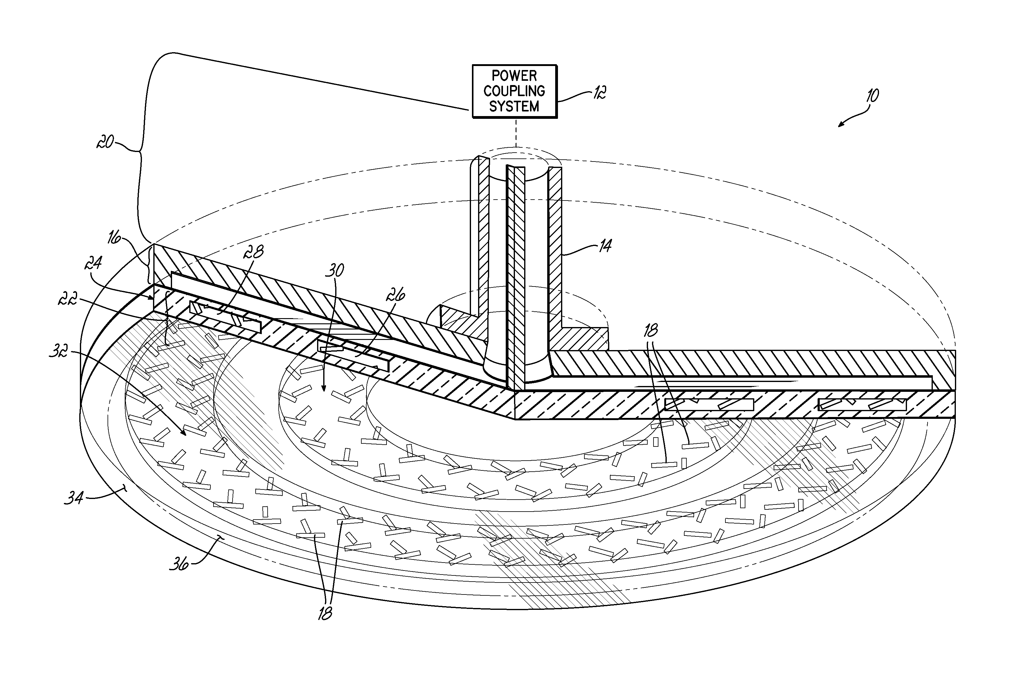
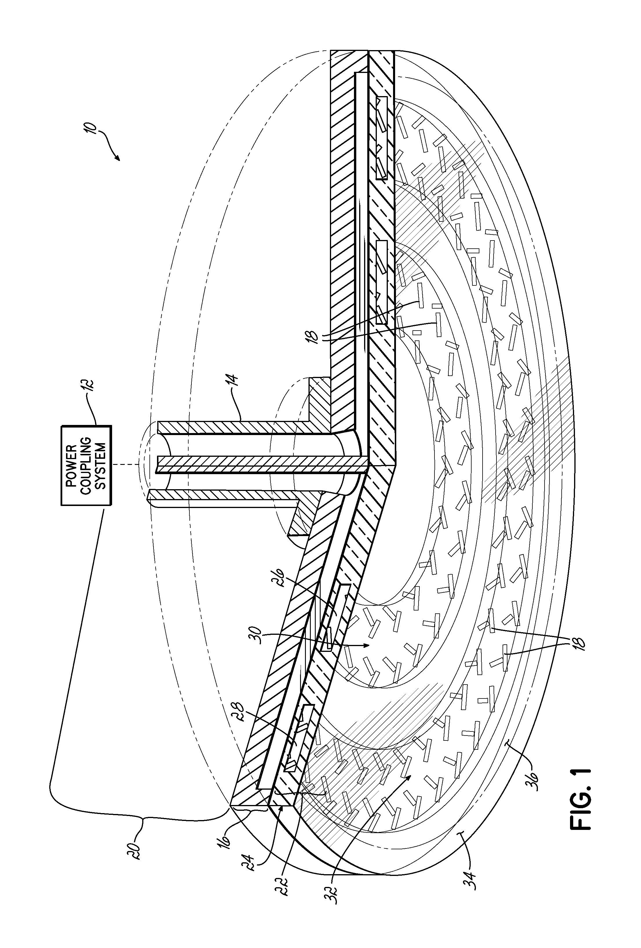
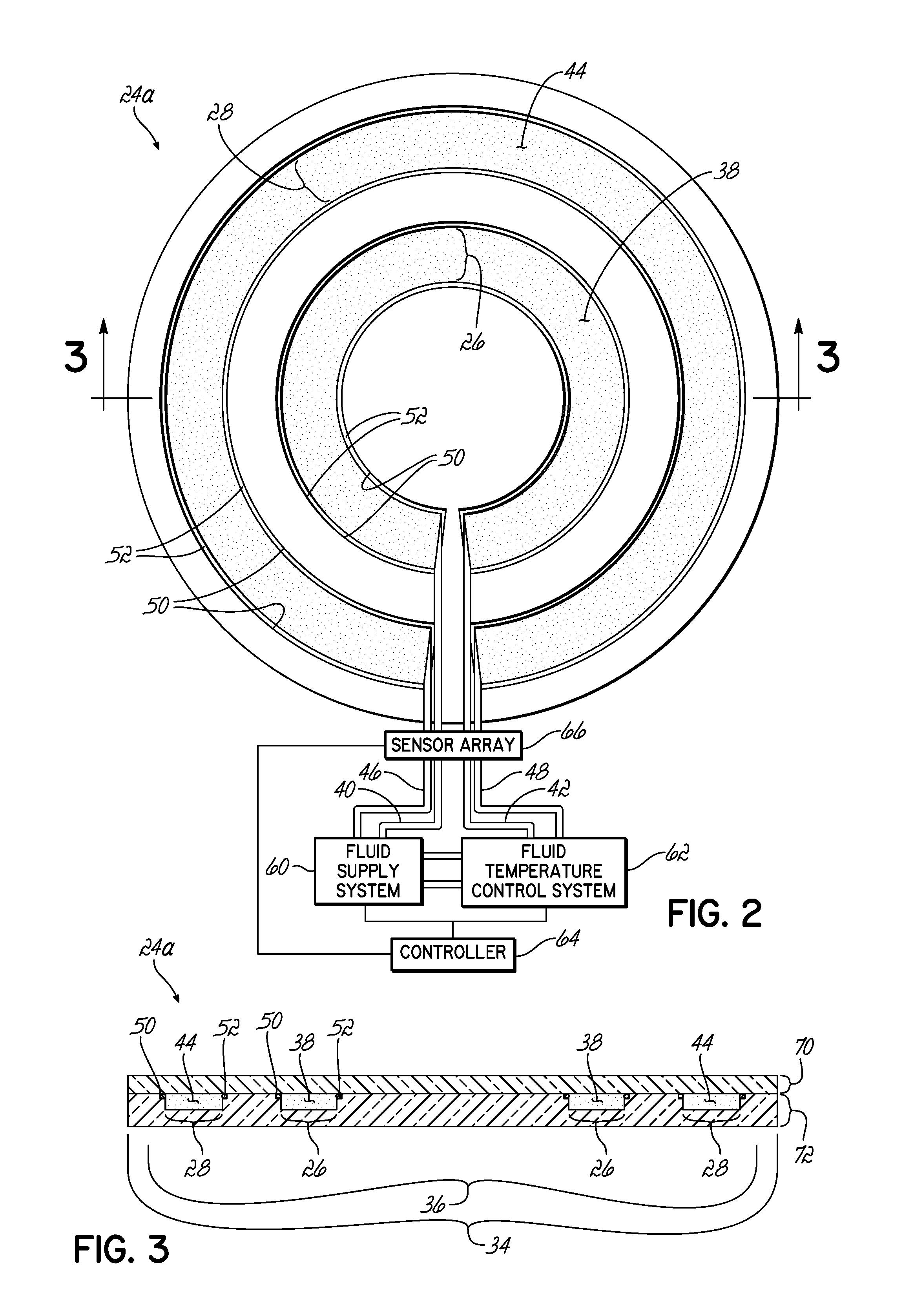
[0015]For more efficient control over plasma density distribution in a processing chamber, the present invention adjusts the microwave power emission from at least one region of slots in a slot antenna assembly of a surface wave plasma source (“SWPS”).

[0016]One of ordinary skill in the art will recognize that the dielectric properties of many liquids change as a function of their temperature. Consequently, the microwave (“MW”) penetration depth (“Dp”) into a liquid can be controlled by changing the temperature of the liquid. The penetration depth Dp can be expressed by the following formula:

Dp=λ02π(2ɛ′)1[{1+(ɛ″ɛ′)2}0.5-1]

wherein ε′ is the relative dielectric constant, ε″ is relative dielectric loss or energy dissipation (ε″ values are higher at lower temperatures), and λ0 is the free space wavelength of the microwave radiation (12.2 cm for 2.45 GHz).

[0017]For example, MW penetration depth Dp in distilled water at 2.45 GHz varies between 1.3 cm and 5 cm when the temperature of the di...


PUM


Abstract

A surface wave plasma source (SWPS) is disclosed, having an electromagnetic (EM) wave launcher including a slot antenna configured to couple EM energy in a desired EM wave mode to a plasma by generating a surface wave on a plasma surface of the SWPS adjacent the plasma. The SWPS also includes a dielectric window positioned below the slot antenna, having a lower surface and the plasma surface. The SWPS further includes an attenuation assembly disposed between the slot antenna and the plasma surface. The attenuation assembly includes a first fluid channel substantially aligned with a first arrangement of slots in the slot antenna, and is configured to receive a first flow of a first fluid at a first fluid temperature. The SWPS finally includes a power coupling system coupled to the EM wave launcher and configured to provide EM energy to the EM wave launcher for forming the plasma.

Description

CROSS REFERENCE TO RELATED APPLICATION[0001]Pursuant to 37 C.F.R. §1.78(a)(4), this application claims the benefit of and priority to prior filed co-pending Provisional Application Ser. No. 61 / 674,941, filed Jul. 24, 2012, which is expressly incorporated herein by reference.FIELD OF THE INVENTION[0002]This invention relates to semiconductor processing technology. Specifically, the invention relates to apparatus and methods for controlling properties of a surface wave plasma source.BACKGROUND OF THE INVENTION[0003]Typically, during semiconductor processing, a (dry) plasma etch process is used to remove or etch material along fine lines or within vias or contacts patterned on a semiconductor substrate. The plasma etch process generally involves positioning a semiconductor substrate with an overlying patterned, protective layer, for example a photoresist layer, into a processing chamber.[0004]Once the substrate is positioned within the chamber, it is etched by introducing an ionizable,...

Claims


Application Information

Patent Timeline
IPC IPC(8): H05H1/46
CPCH05H1/46H05H1/4615H05H1/463
Inventor VORONIN, SERGEY A.RANJAN, ALOK
Owner TOKYO ELECTRON LTD
Why Eureka
Try Eureka