Semiconductor device, and inverter, converter and power conversion device employing the same

Inactive Publication Date: 2014-01-30
SHARP KK
View PDF3 Cites 10 Cited by
  • Summary
  • Abstract
  • Description
  • Claims
  • Application Information

AI Technical Summary

Benefits of technology

[0023]The present semiconductor device includes first and second transistors connected in series between first and second nodes, and a third transistor connected to the second transistor in parallel. The first transistor has first and second electrodes with a higher breakdown voltage therebetween than the second and third transistors do. The second transistor has an amplification factor smaller than that of each of the first and third transistors. The second transistor with the smaller amplification factor ca

Problems solved by technology

Furthermore, the method of PTD 1 requires the same number of current sensors as the high breakdown voltage transistors, each gate resistor to be implemented as a variable resistive eleme

Method used


Image

  • Semiconductor device, and inverter, converter and power conversion device employing the same
  • Semiconductor device, and inverter, converter and power conversion device employing the same
  • Semiconductor device, and inverter, converter and power conversion device employing the same

Examples


Example

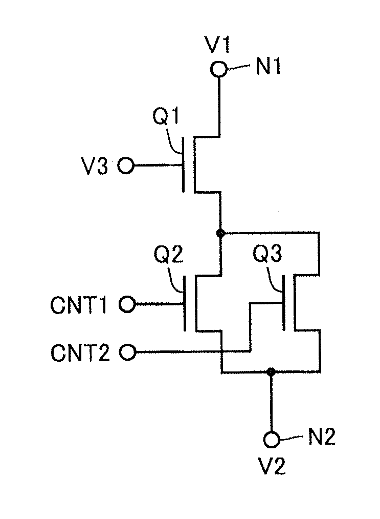
[0043]A first embodiment provides a semiconductor device including: a first transistor having a drain connected to a first node; a second transistor having a drain connected to a source of the first transistor, and a source connected to a second node; and a third transistor connected to the second transistor in parallel, the first transistor having a source-drain breakdown voltage higher than those of the second and third transistors, the second transistor having a transconductance smaller than that of the third transistor. Hereinafter, the semiconductor device of the first embodiment will be described in detail with reference to the drawings.

[0044]As shown in FIG. 1, the semiconductor device of the first embodiment includes n channel MOS transistors Q1 and Q2 connected in series between a node N1 and a node N2, and an n channel MOS transistor Q3 connected to n channel MOS transistor Q2 in parallel.

[0045]Transistor Q1 is a high breakdown voltage transistor, and transistors Q2 and Q3...

Example

Second Embodiment

[0075]FIG. 9 is a circuit diagram showing a configuration of a semiconductor device by a second embodiment of the present invention, as compared with FIG. 1. The FIG. 9 semiconductor device differs from the FIG. 1 semiconductor device in that the former has a normally on type transistor Q4 in place of n channel MOS transistor Q1. Normally on type transistor Q4 is implemented for example as a heterojunction field effect GaN transistor.

[0076]N channel MOS transistor Q1 has threshold voltage VTH1 having a positive value and turns off for a gate-source voltage of 0 V, and accordingly, it is referred to as a normally off type transistor. In contrast, normally on type transistor Q4 has a threshold voltage VTH4 having a negative value and turns on for the gate-source voltage of 0 V. Transistor Q4 is a high breakdown voltage, high Gm transistor.

[0077]Transistor Q4 as commercially available has threshold voltage VTH4 varying within a range of −3 V to −5 V. Transistors Q2 and...

Example

Third Embodiment

[0089]A third embodiment provides a semiconductor device including a plurality of sets of first to third transistors, with a plurality of first transistors having their respective gates connected to each other, a plurality of second transistors having their respective gates connected to each other, a plurality of third transistors having their respective gates connected to each other, the plurality of first transistors having their respective sources all connected to a first node, the plurality of second transistors having their respective sources connected to the plurality of first transistors at their respective drains, respectively, the plurality of second transistors having their respective sources all connected to a second node, and the plurality of third transistors connected to the plurality of second transistors, respectively, in parallel. Hereinafter, the semiconductor device of the third embodiment will be described in detail with reference to the drawings....


PUM


Abstract

A semiconductor device includes a high breakdown voltage, high Gm first transistor and a low breakdown voltage, low Gm second transistor connected in series between first and second nodes, and a low breakdown voltage, high Gm third transistor connected to the second transistor in parallel. When the second transistor is turned on, the first transistor turns on, and furthermore, when the third transistor is turned on, an electrically conducting state is established between the first and second nodes. The second, low breakdown voltage transistor is turned on to turn on the first, high breakdown voltage transistor, and a turn-on time with only limited variation can be achieved.

Description

REFERENCE TO RELATED APPLICATIONS[0001]This application is a national stage application under 35 USC 371 of International Application No. PCT / JP2012 / 059319, filed Apr. 5, 2012, which claims the priority of Japanese Patent Application Nos. 2011-086116, filed Apr. 8, 2011, and 2012-076613, filed Mar. 29, 2012, the entire contents of which are incorporated herein by reference.FIELD OF THE INVENTION[0002]The present invention relates to a semiconductor device, and a boost chopper and power conversion device employing the same, and more specifically to a semiconductor device including a high breakdown voltage transistor, and an inverter, converter and power conversion device employing the same.BACKGROUND OF THE INVENTION[0003]Conventionally, power conversion devices employ a high breakdown voltage transistor. Furthermore, there is also a method using a plurality of high breakdown voltage transistors connected in parallel to allow a power conversion device to have an increased rated curre...

Claims


Application Information

Patent Timeline
IPC IPC(8): H03K17/30
CPCH03K17/302H03K17/102H03K17/122H02M1/088H02M3/158H03K17/145
Inventor KOMIYA, KENJIWAKAIKI, SHUJIKATAOKA, KOHTAROHNOMURA, MASARUOHTA, YOSHIJIIWATA, HIROSHI
Owner SHARP KK
Why Eureka
Try Eureka