Automatic Misalignment Balancing Scheme for Multi-Patterning Technology

a technology of automatic misalignment and multi-patterning, applied in the field of automatic misalignment balancing scheme for multi-patterning technology, can solve the problem that the tool vendor cannot decrease the wavelength of the illumination source,

Active Publication Date: 2014-02-06
TAIWAN SEMICON MFG CO LTD
View PDF0 Cites 17 Cited by
  • Summary
  • Abstract
  • Description
  • Claims
  • Application Information

AI Technical Summary

Problems solved by technology

In recent years however, tool vendors have been unable to decrease the wavelength of illumination sources (e.g., to successfully implement EUV or x-ray lithography), so that developing technology nodes often have minimum feature sizes less than the wavelength of illumination used in exposure tools.

Method used


Image

  • Automatic Misalignment Balancing Scheme for Multi-Patterning Technology
  • Automatic Misalignment Balancing Scheme for Multi-Patterning Technology
  • Automatic Misalignment Balancing Scheme for Multi-Patterning Technology

Examples


Embodiment Construction

[0013]The description herein is made with reference to the drawings, wherein like reference numerals are generally utilized to refer to like elements throughout, and wherein the various structures are not necessarily drawn to scale. In the following description, for purposes of explanation, numerous specific details are set forth in order to facilitate understanding. It may be evident, however, to one of ordinary skill in the art, that one or more aspects described herein may be practiced with a lesser degree of these specific details. In other instances, known structures and devices are shown in block diagram form to facilitate understanding.

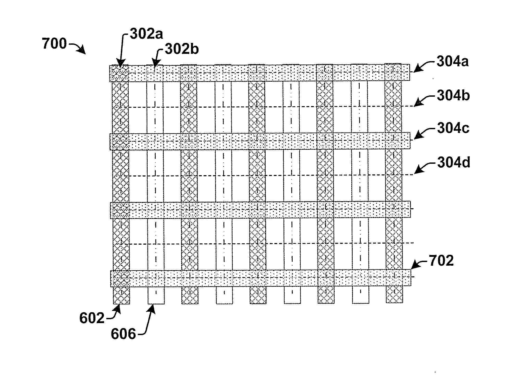
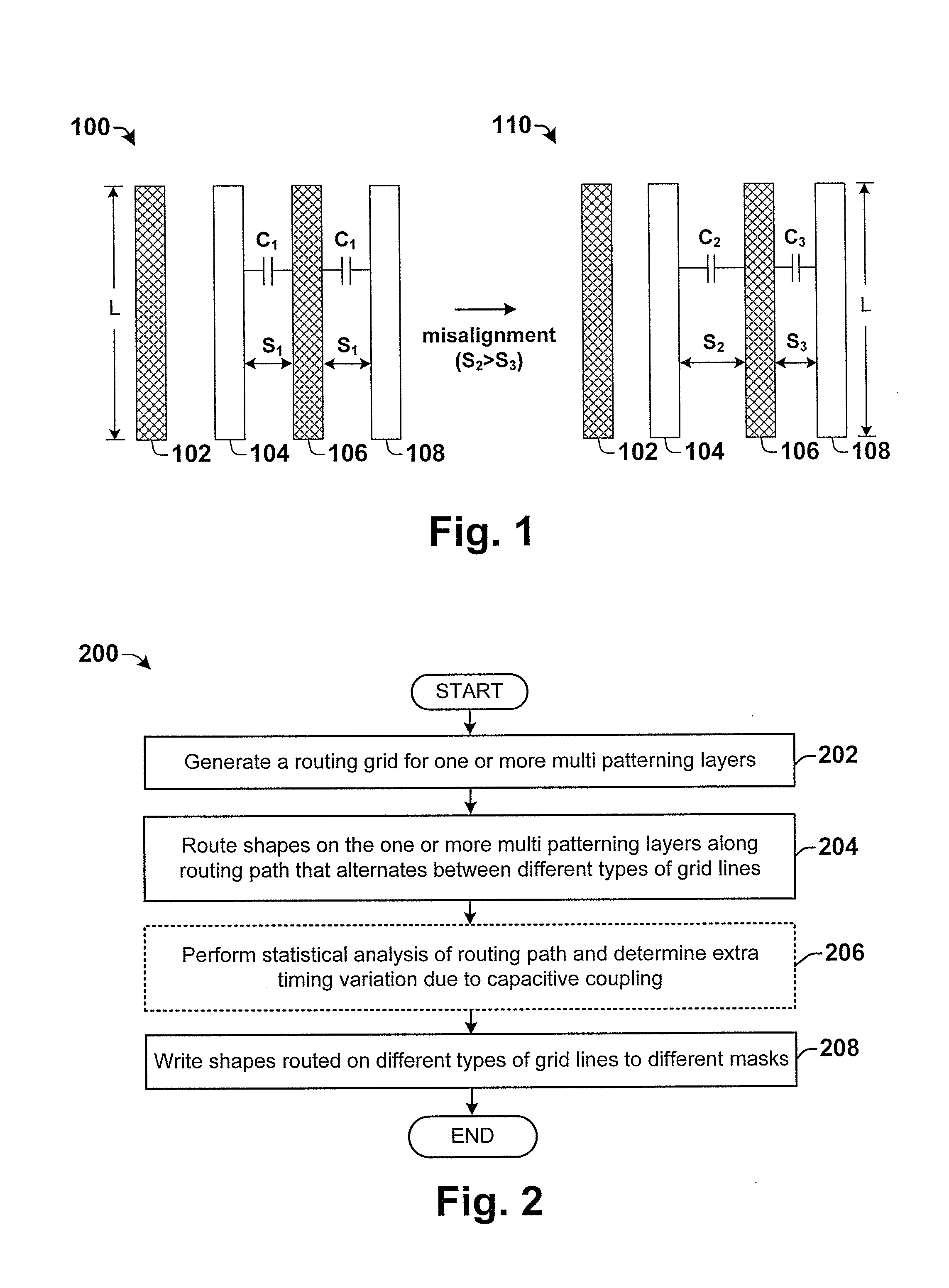
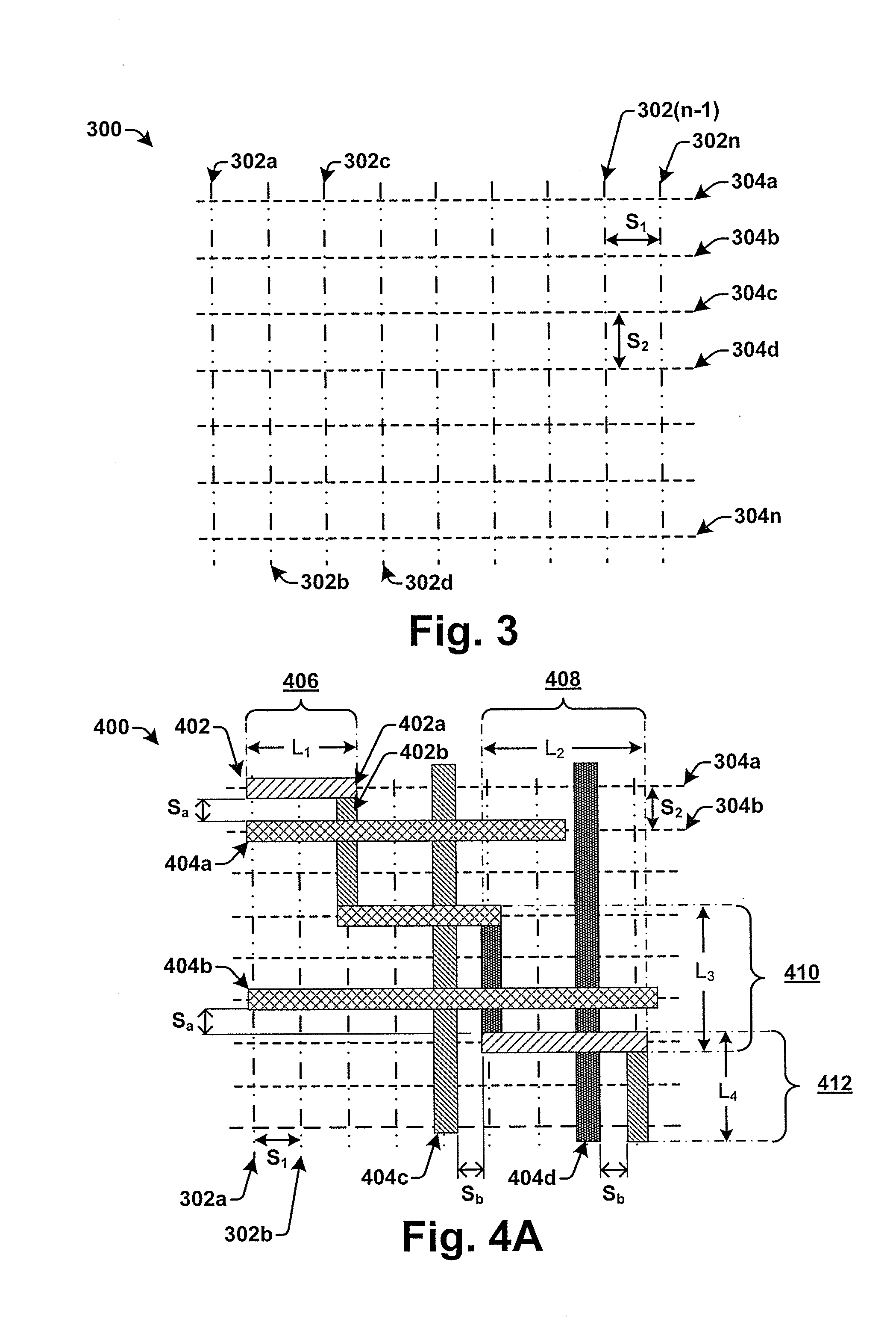
[0014]The use of multiple patterning lithography allows for a lithographic tool to print design features having a minimum feature size smaller than that printable on a single photomask (mask). However, breaking an integrated chip layout onto multiple masks can introduce an overlay error from a misalignment between the masks. FIG. 1 is a block d...


PUM

PropertyMeasurementUnit
dielectric constantaaaaaaaaaa
distanceaaaaaaaaaa

Abstract

Some aspects of the present disclosure provide for a method of automatically balancing mask misalignment for multiple patterning layers to minimize the consequences of mask misalignment. In some embodiments, the method defines a routing grid for one or more double patterning layers within an IC layout. The routing grid has a plurality of vertical grid lines extending along a first direction and a plurality of horizontal grid lines extending along a second, orthogonal direction. Alternating lines of the routing grid in a given direction (e.g., the horizontal and vertical direction) are assigned different colors. Shapes on the double patterning layers are then routed along the routing grid in a manner that alternates between different colored grid lines. By routing in such a manner, variations in capacitive coupling caused by mask misalignment are reduced.

Description

BACKGROUND[0001]Over the last four decades, the semiconductor industry has continually improved the speed and power of integrated chips (ICs) by reducing the size of components within the ICs. In large part, the ability to shrink the size of components within an integrated chip is driven by lithographic resolution. In recent years however, tool vendors have been unable to decrease the wavelength of illumination sources (e.g., to successfully implement EUV or x-ray lithography), so that developing technology nodes often have minimum feature sizes less than the wavelength of illumination used in exposure tools. Therefore, IC fabrication processes have been forced to use tricks (e.g., immersion lithography, dual tone resist, etc.) that improve the resolution of existing lithography tools in a manner that extends their usefulness.[0002]Double patterning lithography (DPL) is one lithography strategy that is used in advanced technology nodes. To perform DPL, an IC layout is decomposed acc...

Claims


Application Information

Patent Timeline
Patent Type & Authority Applications(United States)
IPC IPC(8): G06F17/50G03F1/68
CPCG03F7/70433G03F7/70466G06F30/394
Inventor CHERN, CHAN-HONGCHUNG, TAO WENHUANG, MING-CHIEHLIN, CHIH-CHANGHSUEH, FU-LUNG
Owner TAIWAN SEMICON MFG CO LTD
Why Eureka
Try Eureka