

Semiconductor device and manufacturing method thereof
a semiconductor layer and semiconductor technology, applied in the direction of semiconductor devices, electrical devices, transistors, etc., can solve the problems of low long-term reliability of semiconductors using oxide semiconductor layers and many oxygen vacancies in the manufacturing process, and achieve the effect of preventing a change in electrical characteristics and high reliability
- Summary
- Abstract
- Description
- Claims
- Application Information
AI Technical Summary
Benefits of technology
Problems solved by technology
Method used
Image

Examples
embodiment 1
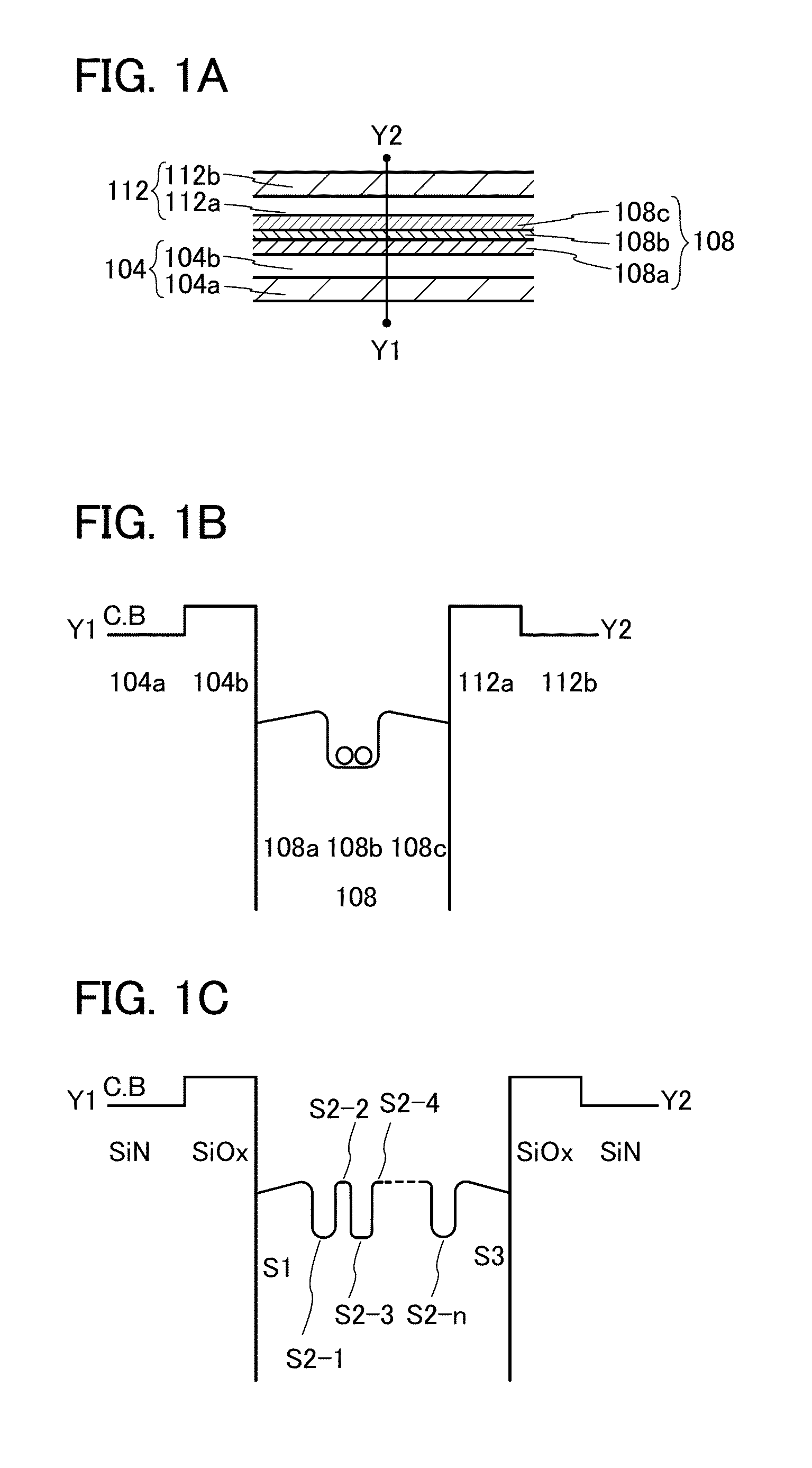
[0043]In this embodiment, a stacked-layer structure included in a semiconductor device of one embodiment of the present invention will be described with reference to FIGS. 1A to 1C.
[0044]FIG. 1A is a conceptual drawing of an example of the stacked-layer structure.
[0045]The stacked-layer structure included in the semiconductor device includes an oxide semiconductor stack 108 between an insulating layer 104 and an insulating layer 112. The oxide semiconductor stack 108 includes at least a first oxide semiconductor layer 108a having an amorphous structure, a second semiconductor layer 108b having a crystalline structure, and a third oxide semiconductor layer 108c.
[0046]In this embodiment, the insulating layer 104 which is placed below the oxide semiconductor stack 108 has a stacked-layer structure of an insulating layer 104a and an insulating layer 104b. Further, the insulating layer 112 which is placed above the oxide semiconductor stack 108 has a stacked-layer structure of an insula...
embodiment 2
[0096]In this embodiment, a transistor is given as an example of the semiconductor device having a stacked-layer structure in Embodiment 1.
[0097]There is no particular limitation on the structure of the transistor that can be applied to a semiconductor device according to one embodiment of the present invention; for example, a staggered type or a planar type having a top-gate structure or a bottom-gate structure can be employed. Further, the transistor may have a single gate structure including one channel formation region, or a multi-gate structure such as a double gate structure including two channel formation regions or a triple gate structure including three channel formation regions. Further, a transistor may have a dual-gate structure including two gate electrodes positioned above and below a channel formation region with gate insulating films provided therebetween.
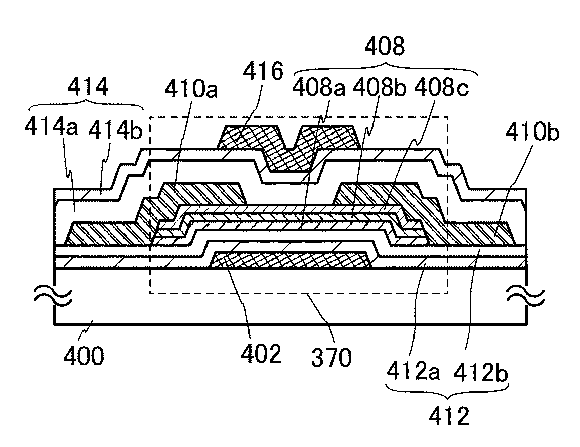
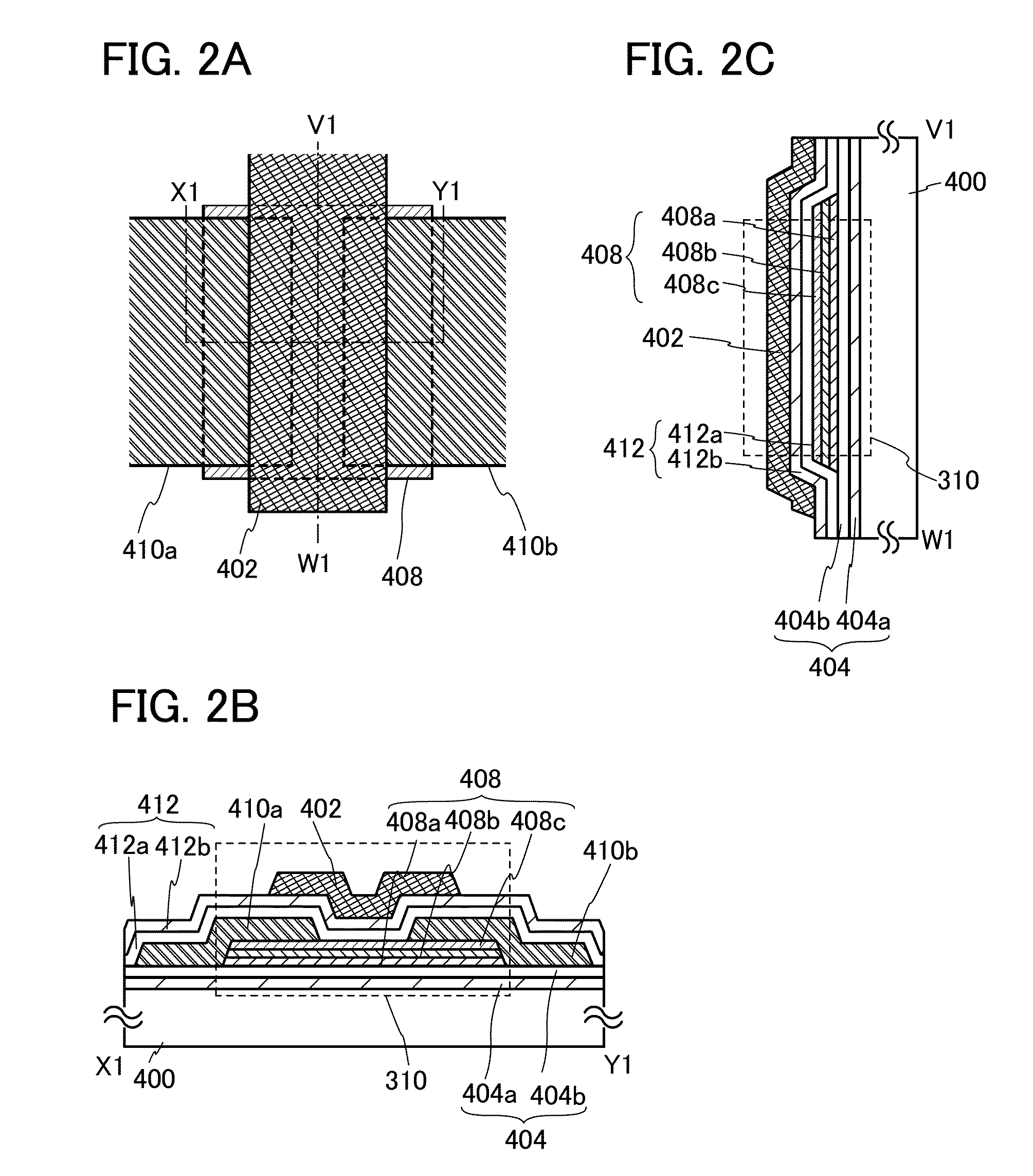
[0098]FIGS. 2A to 2C show a structure example of a top-gate transistor 310. FIG. 2A is a plan view of the transis...
embodiment 3
[0169]In this embodiment, a CAAC-OS layer is described in detail as an example of an oxide semiconductor layer having a crystalline structure which can be used as the second oxide semiconductor layer and / or the third oxide semiconductor layer.
[0170]The CAAC-OS layer is formed using a sputtering target. Here, methods for manufacturing sputtering targets each including an oxide semiconductor having a crystal part in which the direction of the c-axis is parallel to a normal vector of the top surface of the oxide semiconductor will be described (see FIG. 12).
[0171]First, raw materials for the sputtering target are weighed (step S101).
[0172]Here, an InOX raw material (a raw material of In), a GaOY raw material (a raw material of Ga), and a ZnOZ raw material (a raw material of Zn) are prepared as raw materials for the sputtering target. Note that X, Y, and Z are each a given positive number; for example, X, Y, and Z are 1.5, 1.5, and 1, respectively. It is needless to say that the above r...
PUM
 Abstract
Description
Claims
Application Information