
Controllable polarity FET based arithmetic and differential logic

a controllable polarity, differential logic technology, applied in the direction of computation using denominational number representation, pulse technique, instruments, etc., can solve the problems of missing further optimization opportunities, no efficient implementation of unate functions, short circuit current,

Active Publication Date: 2014-02-13
ECOLE POLYTECHNIQUE FEDERALE DE LAUSANNE (EPFL)
View PDF3 Cites 11 Cited by
  • Summary
  • Abstract
  • Description
  • Claims
  • Application Information

AI Technical Summary

Benefits of technology

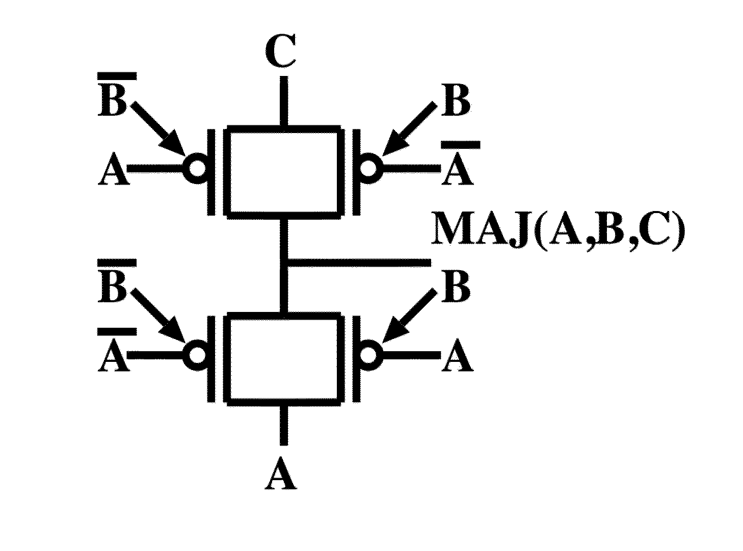
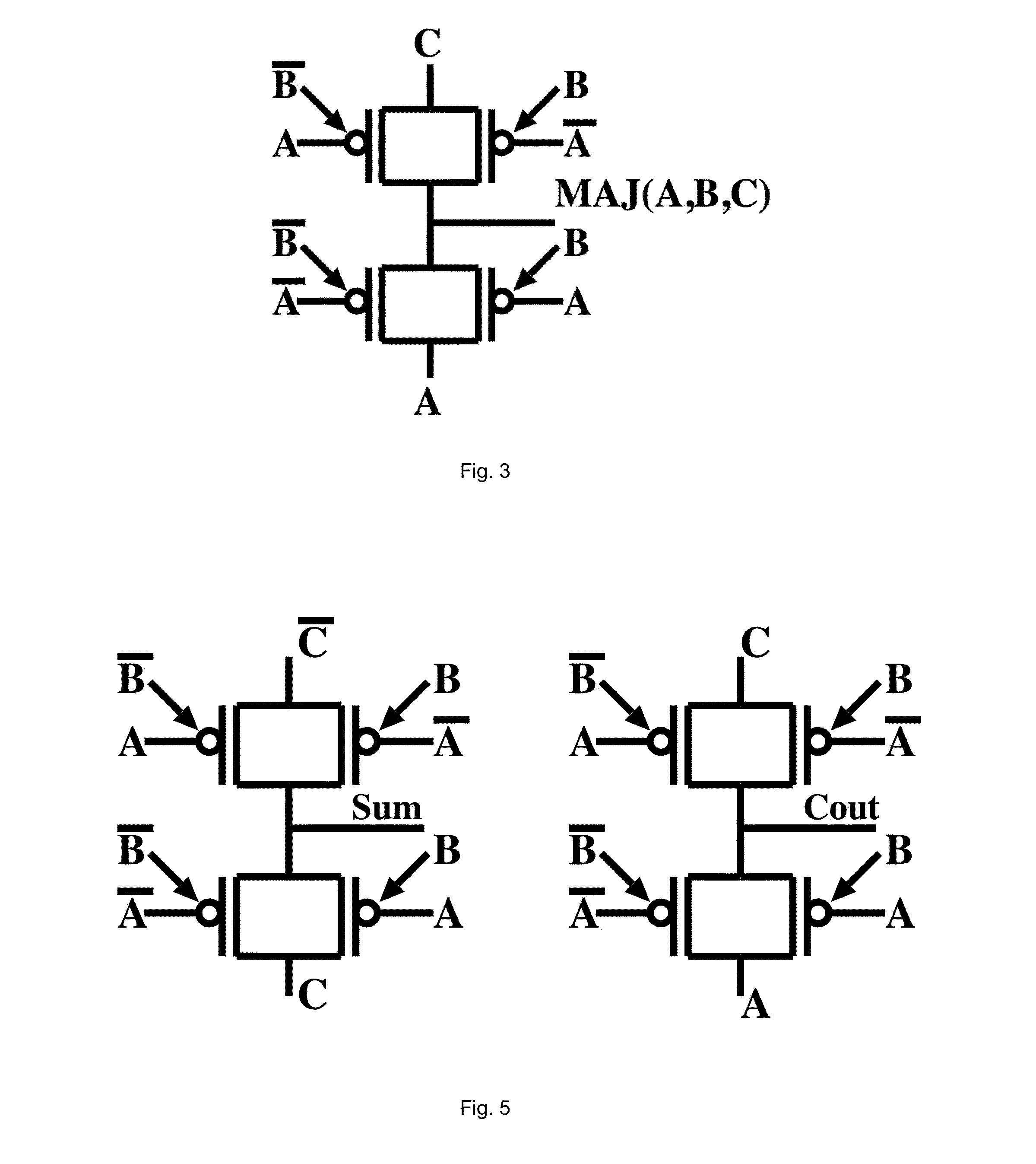
The invention provides logic circuits with three inputs and one output that use a function called MAJ(A,B,C) to combine the inputs. The circuits can use double-gate controllable polarity devices and / or Pass-Gates to route inputs to the output. The circuits can be vertically stacked and sharing the same gate-input signals. The invention also provides a circuit in Differential Cascade Voltage Switch Logic (DCVSL) style that has power gating capabilities and a cascade implementation of power-gated circuits that uses alternating use of the DCVSL circuit and standard non-power-gated DCVSL style circuits.

Problems solved by technology

Despite these gates can be employed to obtain denser and faster circuits, none has been proposed to efficiently implement unate functions in ambipolar technology, missing further optimization opportunities.
However, a critical problem with complementary gates implementing binate functions is the short circuit current.
In addition, the inverter for A affects the overall circuit delay.
However, these advantages are achieved at cost of the extra logic needed to generate complementary inputs.
Power consumption is a serious issue with advanced nano-scale devices.
Among them, ambipolar devices target binate functions (e.g. XOR) that intrinsically have a high switching activity; hence the problem is even exacerbated.
However, power gating presents also drawbacks.
In the active mode, the sleep transistor lowers the supply voltage reducing the logic block performance.
In the standby mode, outputs are floating and may lead to large short circuit currents in successive blocks.

Method used


Image

  • Controllable polarity FET based arithmetic and differential logic
  • Controllable polarity FET based arithmetic and differential logic
  • Controllable polarity FET based arithmetic and differential logic

Examples


Embodiment Construction

Ambipolar Majority Gate

[0039]The present invention concerns a novel 3-input Ambipolar Majority gate. With respect to a novel FinFET realization of the Majority gate in [14], the described Ambipolar Majority gate avoids series stacking of transistors making the relative gate smaller and faster. Moreover, we only need the complementary signals of 2 inputs over 3 while in [14] all the 3 inputs need to be complemented. The description further describes an example embodiment wherein the inventive Ambipolar Majority gate is employed to efficiently design a Full-Adder. The proposed Ambipolar Majority Gate enables an advantageous realization of the Full-Adder with Vertically Stacked Nanowires (VSN).

[0040]The 3-input majority function has the following minimal Sum Of Product (SOP) representation:

Maj(a,b,c)=ab+bc+ac

[0041]This can be rewritten using the XOR operation as:

Maj(a,b,c)=(a⊕b)c+(a⊕b)′a

[0042]With x(a,b)=a⊕b, it becomes

Maj(a,b,c)=x(a, b)c+x(a, b)′a

[0043]This form suggests to use a C...


PUM


Abstract

A logic gate with three inputs A, B, and C, and one output implementing a function MAJ(A,B,C)=A*B+B*C+A*C comprising two mutually exclusive transmission gates (TGs) connected in series, based on two parallel double-gate controllable polarity devices, a polarity of each being controlled by input A and a conduction being controlled by input B, or vice-versa, in opposite polarities, and that route either an input A or C from one side of the transmission gates to the output.

Description

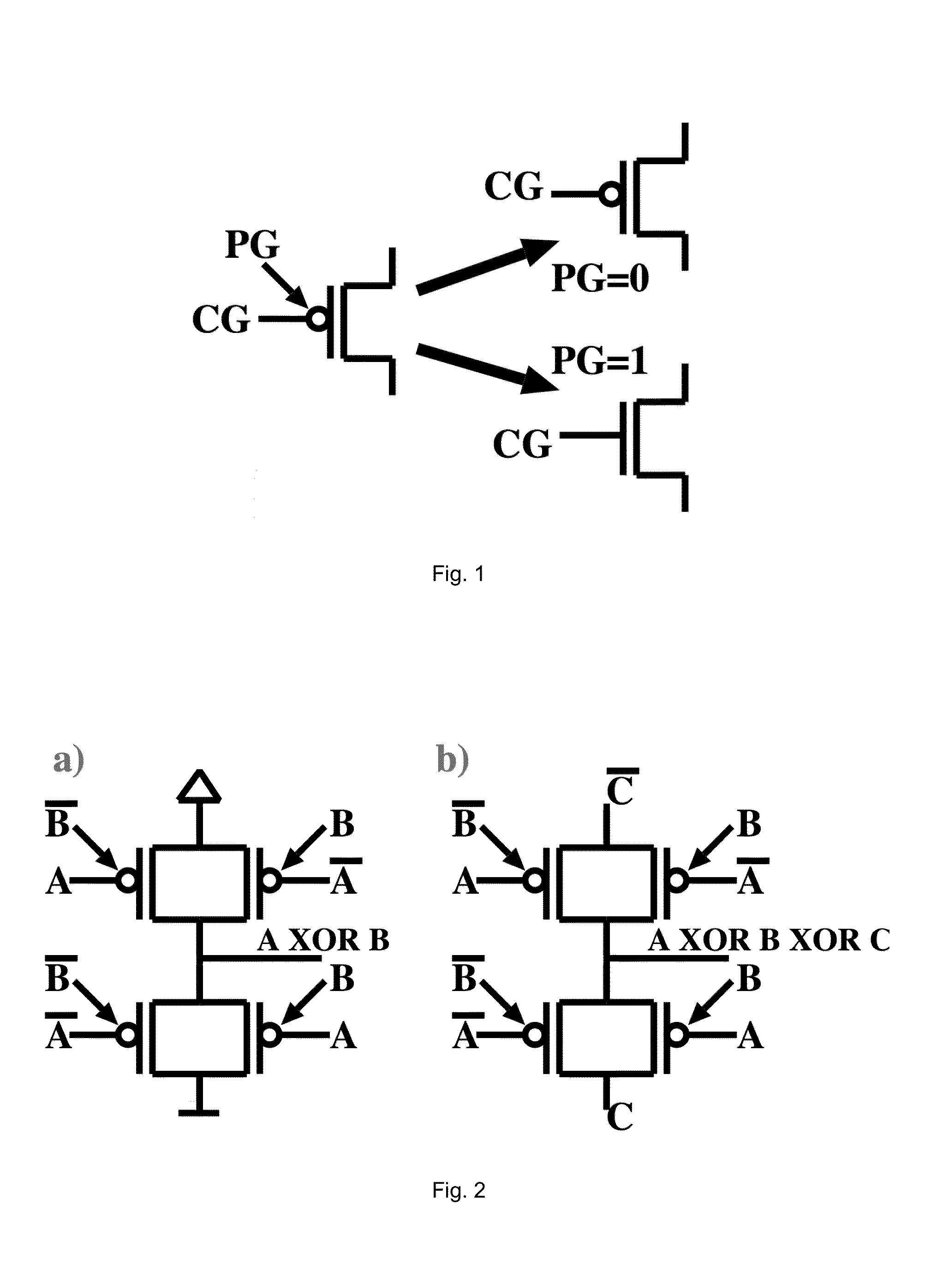
CROSS-REFERENCE TO RELATED APPLICATIONS[0001]This application claims the benefit of European Patent Application No. 12179928.2 filed Aug. 9, 2012, the entire disclosure of which is incorporated herein by reference.TECHNICAL FIELD[0002]The invention relates to a majority logic gate based on double-gate controllable polarity Field Effect Transistors (FETs).[0003]The invention further relates to Differential Cascade Voltage Switch Logic (DCVSL) style, which finds use with double-gate controllable polarity Field Effect Transistors (FETs).BACKGROUND[0004]Ambipolar transistors are Double Independent Gate (DIG) FETs with device polarity controllable via the second gate. DIG ambipolar FETs have been reported in many nano-scale emerging technologies [1]-[5], [13]. In FIG. 1, the polarity control operation is shown: the Polarity Gate (PG) set the device polarity while the Conventional Gate (CG) set the on-state in the usual way.[0005]Recently, several works have proved that DIG ambipolar FETs...

Claims


Application Information

Patent Timeline
IPC IPC(8): H03K19/23H03K17/687H03K19/21
CPCH03K19/23H03K17/687H03K19/215H03K19/20
Inventor AMARU, LUCA GAETANOGAILLARDON, PIERRE-EMMANUEL JULIEN MARCDE MICHELI, GIOVANNI
Owner ECOLE POLYTECHNIQUE FEDERALE DE LAUSANNE (EPFL)
Learn More