
Method for cleaning semiconductor wafer

Active Publication Date: 2014-02-20
SHIN-ETSU HANDOTAI CO LTD
View PDF1 Cites 4 Cited by
  • Summary
  • Abstract
  • Description
  • Claims
  • Application Information

AI Technical Summary

Benefits of technology

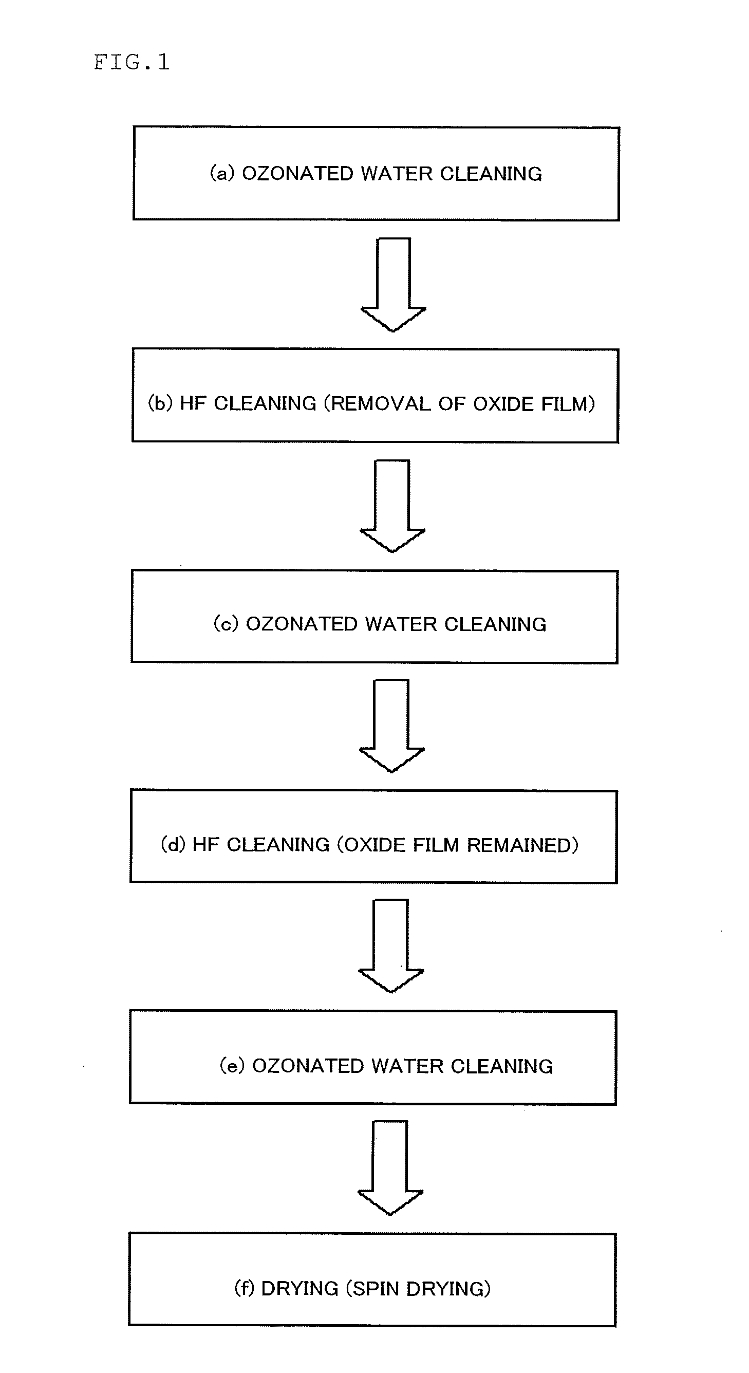
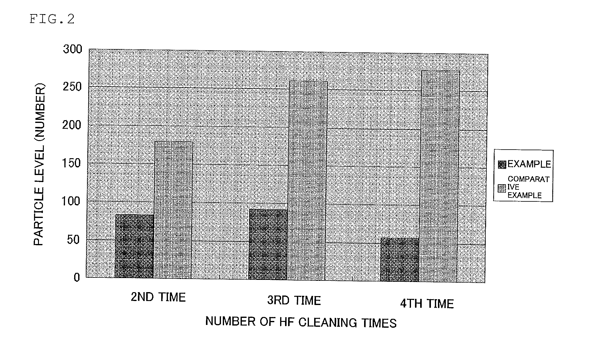
The present invention is a method for cleaning semiconductor wafers that can effectively and conveniently reduce particles on the surface of the wafer and simultaneously reduce metal impurities and particle levels.

Problems solved by technology

Therefore, in the cleaning of a semiconductor wafer, it is the problem to reduce the metal impurity level and the particle level simultaneously.

Method used


Image

  • Method for cleaning semiconductor wafer
  • Method for cleaning semiconductor wafer

Examples


example 1

[0040]First, 15 wafers of silicon single crystal wafers having a diameter of 300 mm and both surfaces of which are mirror polished to have clean surfaces were prepared. Next, 3 wafers of the silicon single crystal wafers among the 15 wafers having clean surfaces were pulled out, and one of which was subjected to particle measurement by a wafer surface defect testing equipment (Particle counter, LS-6800 (≧41 nm) product of Hitachi High-Technologies Corporation) to examine the particle level before cleaning. As a result of the measurement, it could be found out that the wafer particle level before the cleaning was good level of 100 particles or less. Also, to examine concentrations of metal impurities attached to the surface before cleaning, 2 wafers thereof were subjected to vapor phase decomposition of a natural oxide film at the wafer surface by HF vapor, and then, the metal impurities on the wafer surface were recovered by HF liquid drops, and measurement of the concentrations of ...

example 2

[0046]Among the silicon single crystal wafers prepared in Example 1, 2 wafers thereof were subjected to cleaning as mentioned below, and measurement of the particle level and metal impurity level were carried out.

[0047]As shown in Table 1, cleaning of the silicon single crystal wafer was carried out in the same manner as in Example 1 except that the cleaning was carried out by repeating the ozonated water cleaning after the HF cleaning three times, where the oxide film formed on the surface of the silicon single crystal wafer was entirely removed at the first time HF cleaning, and in all the HF cleanings at the second time or later, the oxide film on the surface of the silicon single crystal wafer by the ozonated water cleaning was not entirely removed to remain a part of the thickness thereof on the surface of the silicon single crystal wafer.

[0048]Measurement of the particle level and the metal impurity level at the surface of the silicon single crystal wafer thus subjected to cle...

example 3

[0049]Among the silicon single crystal wafers prepared in Example 1, 2 wafers thereof were subjected to cleaning as mentioned below, and measurement of the particle level and metal impurity level were carried out.

[0050]As shown in Table 1, cleaning of the silicon single crystal wafer was carried out in the same manner as in Example 1 except that the cleaning was carried out by repeating the ozonated water cleaning after the HF cleaning four times, where the oxide film formed on the surface of the silicon single crystal wafer was entirely removed at the first time HF cleaning, and in all the HF cleanings at the second time or later, the oxide film on the surface of the silicon single crystal wafer by the ozonated water cleaning was not entirely removed to remain a part of the thickness thereof on the surface of the silicon single crystal wafer.

[0051]Measurement of the particle level and the metal impurity level at the surface of the silicon single crystal wafer thus subjected to clea...


PUM

PropertyMeasurementUnit
Fractionaaaaaaaaaa
Thicknessaaaaaaaaaa
Concentrationaaaaaaaaaa

Abstract

The present invention provides a method for cleaning a semiconductor wafer, in which the method includes cleaning steps of HF cleaning, ozonated water cleaning and HF cleaning in this order at least one time, wherein in the HF cleaning carried out last in the method for cleaning the semiconductor wafer, cleaning is so carried out that an oxide film formed on a surface of the semiconductor wafer by the ozonated water is not entirely removed and to remain a part of a thickness thereof on the surface of the semiconductor wafer. As a result, a method for cleaning a semiconductor wafer in which a metal impurity level and a particle level can be reduced simultaneously in the cleaning of the semiconductor wafer is provided.

Description

TECHNICAL FIELD[0001]The present invention relates to a method for cleaning semiconductor wafer.BACKGROUND ART[0002]As one of the cleaning methods of the semiconductor wafer, it has been carried out a cleaning treatment by using ozonated water, diluted hydrofluoric acid, and pure water in combination. As a general flow of the cleaning in this case, the cleaning is carried out in the order of ozonated water cleaning→diluted hydrofluoric acid cleaning→ozonated water (pure water) cleaning→drying.[0003]In this method, an organic material(s) attached to a surface of the semiconductor wafer is removed by the first ozonated water cleaning, an oxide film formed on the surface of the semiconductor wafer and metal impurities incorporated into the oxide film are simultaneously removed in the next diluted hydrofluoric acid cleaning, thereafter, when a protective oxide film is necessary for the surface of the semiconductor wafer, surface oxidation treatment by ozonated water (or pure water) is c...

Claims


Application Information

Patent Timeline
IPC IPC(8): H01L21/02
CPCH01L21/02052C23G1/02H01L21/02H01L21/02041H01L21/304H01L21/4892
Inventor ABE, TATSUOKABASAWA, HITOSHI
Owner SHIN-ETSU HANDOTAI CO LTD
Learn More