Micro-balance sensor integrated with atomic layer deposition chamber

a micro-balance sensor and atomic layer deposition technology, applied in chemical vapor deposition coating, metal material coating process, coating, etc., can solve the problems of inability to achieve accurate measurements of tiny changes in mass during ald, inability to achieve tight temperature control, and inability to reduce temperature-induced variations from mass balances. , to achieve the effect of reducing the modification of the ald instrument, facilitating installation and minimal disruption of the ald process

Active Publication Date: 2014-02-27
UCHICAGO ARGONNE LLC
View PDF12 Cites 62 Cited by
  • Summary
  • Abstract
  • Description
  • Claims
  • Application Information

AI Technical Summary

Benefits of technology

[0017]Another object of the present invention is to integrate oscillating crystal microbalances with ALD equipment. A feature of the invention is that the device has a small “foot print” to permit easy installation through small aperturea in the wall of the reactor of the ALD tool. An advantage of the invention is installation can be achieved with minimal modification of the ALD instrument, and minimal disruption to the ALD process. The feature facilitates the installation of a plurality of crystals in the ALD reaction chamber to enable high resolution mapping of several locations of the film being produced.
[0018]Another object of the present invention is to reduce measurement errors and potential electrical shorting that may result from a deposition on the unintended side of the crystal exposed to an ALD reaction environment. A feature of the invention is to provide pressure balancing on a first surface of a mass microbalance while inhibiting flow of deposition moieties to all other surfaces of the microbalance. An advantage of the invention is simultaneously limiting access for deposition to only one crystal surface while maintaining the entire crystal under reaction conditions of the deposition reaction chamber.
[0019]Another object of the invention is to permit oscillating crystal microbalances to be operated in an ALD reaction chamber, over a temperature range of between about 25° C. and 300° C. A feature of the invention is to expose the crystal to an ALD deposition environment (including reaction pressures and temperatures) while providing a structure to dissipate heat in a manner that minimizes temperature fluctuations across the crystal. An advantage is that the crystal is located in or adjacent to the ALD environment thereby providing a means to rapidly equilibrate the QCM with the ALD environment in a period of as little as 20 minutes. This minimizes temperature fluctuations and also minimizes the time delay between introducing a substrate into the ALD reactor and achieving a sufficiently stable QCM baseline signal to begin ALD growth and thickness measurement.
[0020]In brief, the invention provides a device for measuring deposition rate of a substance onto a substrate, the device comprising a reaction chamber; an aperture in the chamber; a piezoelectric element within the aperture, whereby a first region of the piezoelectric element is in fluid communication with the chamber and the second region is isolated from the chemical reactants in the reaction chamber; a means for equalizing pressure between said first region and a second region of the piezoelectric element; a means to induce oscillation of the piezoelectric element at a first frequency wherein a change in the oscillation of the piezoelectric element is proportional to the deposition of the substance on the first region of the piezoelectric element.
[0021]The invention provides a device and process for measuring deposition rates in an ALD with minimal modification to the ALD device.

Problems solved by technology

Often, volatile by-products are produced.
Obtaining accurate measurements of tiny changes in mass during ALD is difficult because state of the art microbalances, such as those utilizing oscillating crystal paradigms, are intended to be operated at room temperature.
Tight temperature control, e.g., with PID controllers to reduce temperature-induced variations from the mass balance, may not always be practical.
Moreover, thermal transients induced by the ALD precursor exposures cannot be eliminated even using PID temperature controllers.
Accurately estimating the mass deposited during ALD is further complicated by deposition on both the front and back of the oscillating crystal—an inevitable consequence of the self-limiting surface chemistry.
Several shortcomings limit the utility of oscillating crystal systems for ALD.
First, temperature equilibration of conventional QCM sensor heads (i.e., fixture on a stick configurations) requires several hours.
This, combined with a significant disturbance of the gas flow dynamics produced by conventional QCM sensor heads, precludes the technique as a routine in situ “monitor” of thickness for co-deposited samples of interest.

Method used


Image

  • Micro-balance sensor integrated with atomic layer deposition chamber
  • Micro-balance sensor integrated with atomic layer deposition chamber
  • Micro-balance sensor integrated with atomic layer deposition chamber

Examples


example

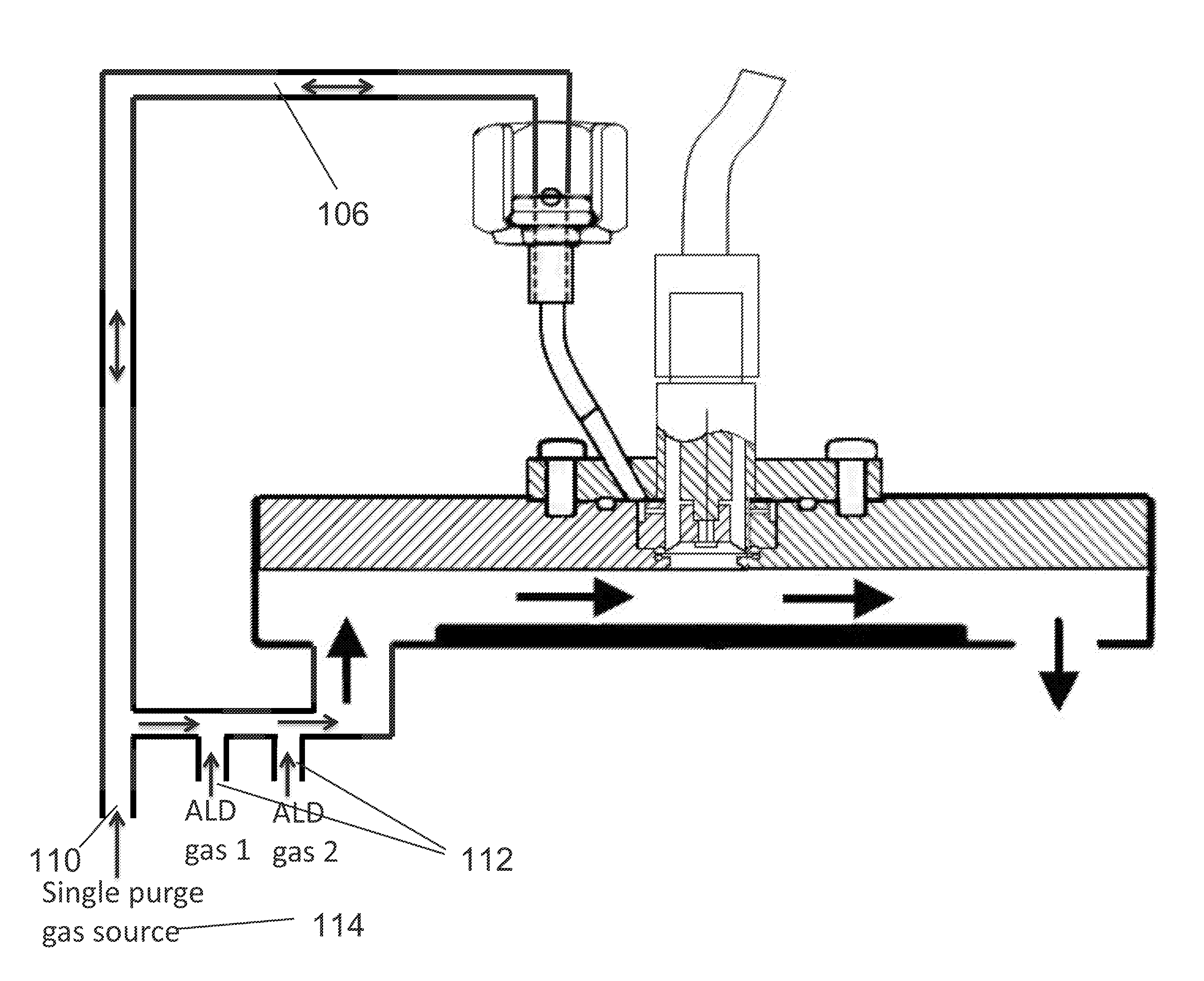
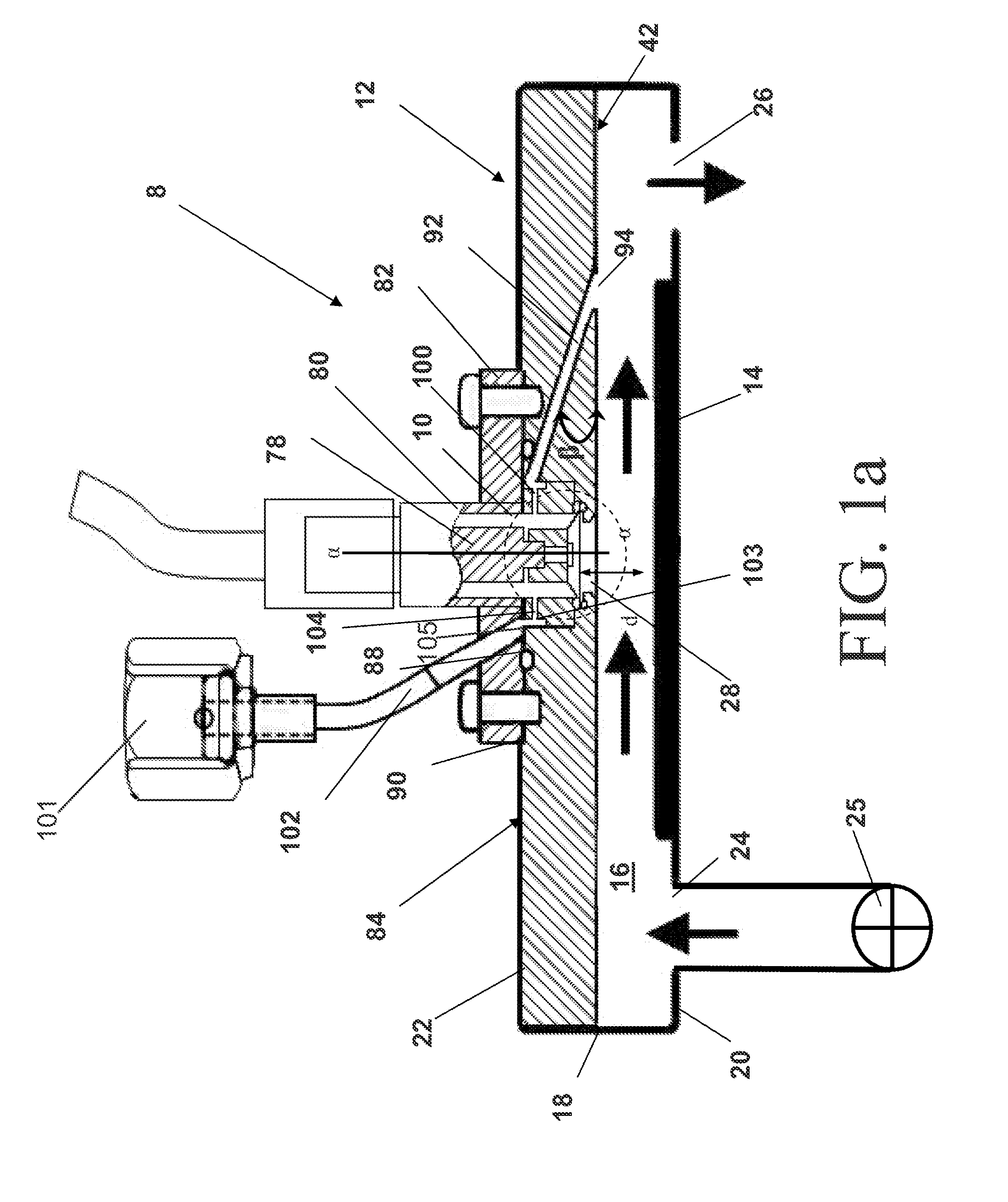
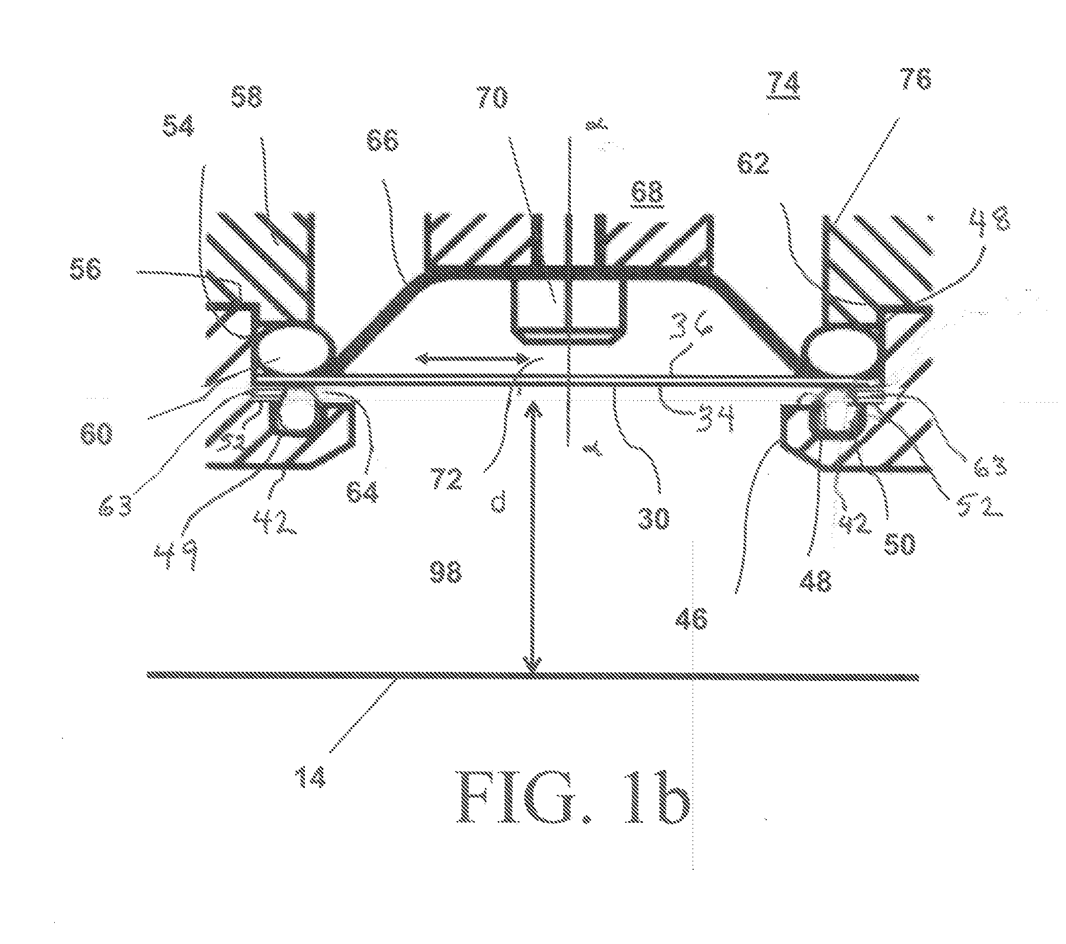
[0083]To illustrate the application of the integral QCM design, of the invention, a commercially available aluminum slab lid of an ALD (for example, a Savannah 200 ALD (Cambridge Nanotech, Inc., Cambridge, Mass.) was modified to accommodate two oscillating crystal fixtures. Compression seal sleeves and apertures were machined to appropriate dimensions to produce O-ring compression compatible with published O-ring specifications and QCM crystal thickness.

[0084]Electrical connection to the front of the gold plated QCM crystals is achieved through direct contact with the aluminum ALD lid by means of edge 52, which is in turn grounded to the Connector shield by the feed through. Electrical connection to the exterior surface of the QCM crystal was achieved with a resilient / spring retainer electrode modified and fitted on a connector shaft. The connector fixture was bolted onto the lid with mounting plate and fasteners were inserted in drilled and tapped holes. Tightening of the fasteners...


PUM

PropertyMeasurementUnit
temperaturesaaaaaaaaaa
thicknessaaaaaaaaaa
temperature coefficientaaaaaaaaaa

Abstract

The invention is directed to QCM measurements in monitoring ALD processes. Previously, significant barriers remain in the ALD processes and accurate execution. To turn this exclusively dedicated in situ technique into a routine characterization method, an integral QCM fixture was developed. This new design is easily implemented on a variety of ALD tools, allows rapid sample exchange, prevents backside deposition, and minimizes both the footprint and flow disturbance. Unlike previous QCM designs, the fast thermal equilibration enables tasks such as temperature-dependent studies and ex situ sample exchange, further highlighting the feasibility of this QCM design for day-to-day use. Finally, the in situ mapping of thin film growth rates across the ALD reactor was demonstrated in a popular commercial tool operating in both continuous and quasi-static ALD modes.

Description

CONTRACTUAL ORIGIN OF THE INVENTION[0001]The U.S. Government has rights in this invention pursuant to Contract No. DE-AC02-06CH11357 between the United States Government and UChicago Argonne, LLC, representing Argonne National Laboratory.FIELD OF THE INVENTION[0002]The present invention relates to the field of atomic layer deposition (ALD), and more particularly, this invention relates to a device and method for quantitatively monitoring ALD film thicknesses during their formation.BACKGROUND OF THE INVENTION[0003]Vapor deposition, in particular physical vapor deposition (PVD) and chemical vapor deposition (CVD), comprises low pressure processes to condense and deposit vaporized material onto workpiece surfaces. PVD involves purely physical processes such as high temperature vacuum evaporation followed by condensation, or plasma sputter bombardment.[0004]CVD employs chemical reactions to produce high-purity, high-performance solid materials. The process is used in semiconductor manuf...

Claims


Application Information

Patent Timeline
Patent Type & Authority Applications(United States)
IPC IPC(8): C23C16/44C23C16/50
CPCC23C16/45525C23C16/52
Inventor MARTINSON, ALEX B. F.LIBERA, JOSEPH A.ELAM, JEFFREY W.RIHA, SHANNON C.
Owner UCHICAGO ARGONNE LLC
Why Eureka
Try Eureka