Lead-free solder bump bonding structure

Active Publication Date: 2014-02-27
NIPPON MICROMETAL
View PDF4 Cites 42 Cited by
  • Summary
  • Abstract
  • Description
  • Claims
  • Application Information

AI Technical Summary

Benefits of technology

This patent describes an invention that relates to improving electrical connections in electronic components. The invention uses lead-free solder bumps to bond together copper electrodes on different components. The patent describes a specific test circuit that was used to evaluate the performance of the solder bumps. The test circuit included eight solder bumps that were arranged in various ways. The results of the test showed that the solder bumps had good electrical characteristics and were resistant to a process called electromigration. This invention can help improve the reliability and durability of electronic components.

Problems solved by technology

In the bonded part of electronic components by a lead-free solder alloy (hereinafter, sometimes simply referred to as a lead-free solder bonded part), however, when a flowing current per a unit area (current density) increases, an electromigration of Cu at the lead-free solder bonded part (hereinafter, electromigration means the electromigration of Cu) occurs, resulting in a disconnection failure in some cases.
Hence, the manufacturing process of the lead-free solder bump bonding structure becomes complex by what corresponds to the necessity of the Ni layer forming process, and thus the increase of the burden like the cost increase at the time of manufacturing is a technical disadvantage.

Method used


Image

  • Lead-free solder bump bonding structure
  • Lead-free solder bump bonding structure
  • Lead-free solder bump bonding structure

Examples


example

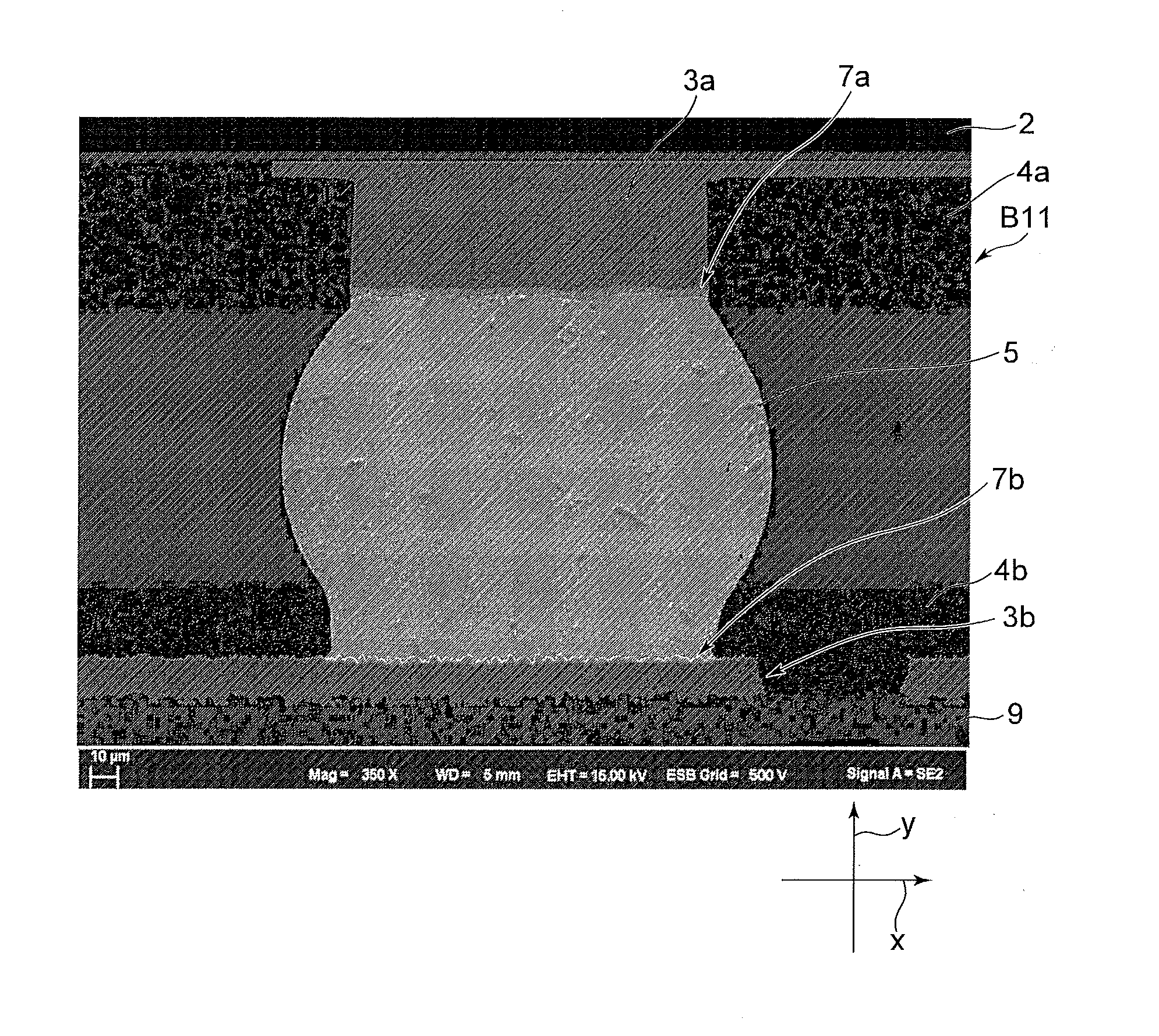
[0094]An explanation will be below given of examples. In this explanation, as illustrated in FIG. 8, a test circuit 21 electrically connected with eight lead-free solder bump bonding structures B11 to B41, B12 to B42 was prepared, and an interface shape of an IMC interface in the lead-free solder bump bonding structure B11 and the anti-electromigration characteristic of the lead-free solder bump bonding structures B11 to B41 and B12 to B42 were tested. According to the test circuit 21, the Cu electrode 3a of the first electronic component 2 and the Cu electrode 3b of the second electronic component 9 were bonded together by multiple lead-free solder bumps 5 to form a total of eight lead-free solder bump bonding structures B11 to B41, and B12 to B42 that were four by two at a center region. Note that reference numeral 25 in FIG. 8 denotes a thermocouple element.

[0095]According to the test circuit 21 of the example 1, a wafer-level package (WLP) cut out from an Si chip was used as the...


PUM


Abstract

According to a lead-free solder bump bonding structure, by causing the interface (IMC interface) of the intermetallic compound layer at a lead-free-solder-bump side to have scallop shapes of equal to or less than 0.02 [portions / μm] without forming in advance an Ni layer as a barrier layer on the surfaces of respective Cu electrodes of first and second electronic components like conventional technologies, a Cu diffusion can be inhibited, thereby inhibiting an occurrence of an electromigration. Hence, the burden at the time of manufacturing can be reduced by what corresponds to an omission of the formation process of the Ni layer as a barrier layer on the Cu electrode surfaces, and thus a lead-free solder bump bonding structure can be provided which reduces a burden at the time of manufacturing in comparison with conventional technologies and which can inhibit an occurrence of an electromigration.

Description

BACKGROUND OF THE INVENTION[0001]1. Field of the Invention[0002]The present invention relates to a lead-free solder bump bonding structure, and is suitable when applied to a lead-free solder bump bonding structure that has, for example, a copper electrode (hereinafter, referred to as a Cu electrode) of a first electronic component and a Cu electrode of a second electronic component bonded by a lead-free solder bump.[0003]2. Description of the Related Art[0004]An example known technique of electrically connecting electronic components of an electronic device, etc., is to utilize a protrusion formed on an electrode and called a bump. In recent years, in view of environmental problems and the RoHS instruction (Restriction of the Use of Certain Hazardous Substances in Electrical and Electronic Equipment) by EU, etc., bumps formed on Cu electrodes employ a lead-free solder alloy containing no Pb (see, for example, JP H05-50286 A).[0005]Moreover, in accordance with the downsizing of elect...

Claims


Application Information

Patent Timeline
IPC IPC(8): H01L23/498
CPCH01L23/49811H01L23/49866B23K2101/36B23K2101/40B23K2101/42B23K35/262H05K3/3463H05K3/3436H05K2201/0769H05K2203/041H01L2224/81948H01L2224/03828H01L24/05H01L24/11H01L24/13H01L24/16H01L24/81H01L2224/0381H01L2224/0401H01L2224/05647H01L2224/05655H01L2224/1132H01L2224/11334H01L2224/1134H01L2224/11849H01L2224/119H01L2224/13111H01L2224/16227H01L2224/81024H01L2224/81191H01L2224/81447H01L2224/81815H01L2924/301H01L2224/81048H01L2224/11848H01L2224/16503B23K35/0244B23K35/025H01L23/49816H01L2924/381H01L2224/16225H01L2924/01028H01L2924/01029H01L2924/01047H01L2924/01027H01L2924/01026H01L2924/01015H01L2924/01012H01L2924/01032H01L2924/01046H01L2924/01025H01L2924/01013H01L2924/01051H01L2924/01049H01L2924/0103H01L2924/00014H01L2924/00012H01L2924/00015
Inventor HASHINO, EIJIISHIKAWA, SHINJITERASHIMA, SHINICHITANAKA, MASAMOTO
Owner NIPPON MICROMETAL
Why Eureka
Try Eureka