Terminal structure and semiconductor device

a technology of terminal structure and semiconductor device, which is applied in the direction of semiconductor device, semiconductor/solid-state device details, electrical apparatus, etc., can solve the problems that the use of the aforementioned conventional bumps cannot meet the need for bump pitch reduction, limits the potential bump pitch reduction, and the bump base portion may not be sufficiently wrapped around the bump base portion at mounting, so as to suppress the risk of bump shorting, the effect of bump pitch

Active Publication Date: 2014-02-27
TDK CORPARATION
View PDF6 Cites 5 Cited by
  • Summary
  • Abstract
  • Description
  • Claims
  • Application Information

AI Technical Summary

Benefits of technology

[0012]Also, in the present invention, the bump preferably has a maximum diameter of 5 to 40 μm. This makes it possible to more suppress a risk of shorting of bumps to each other even if the bump pitch is reduced.
[0013]Also, in the present invention, the bump preferably contains tin (Sn) as a main component. This causes the bump to have a suitable dome shape, leading to that the height at which the bump has a maximum diameter can be easily located lower than the maximum height of the under-bump metal layer. As used herein, “contains tin as a main component” means that the content of tin is 90 mass % or more of the entire constituent component.
[0014]Also, in the present invention, the under-bump metal layer preferably contains nickel (Ni) as a main component. This makes it possible to suitably suppress the metal contained in the bump from diffusing into the external electrode. As used herein, “contains nickel as a main component” means that the content of nickel is 85 mass % or more of the entire constituent component.
[0015]Further, in the present invention, the bump preferably contains titanium (Ti). This makes it possible to suitably suppress the metal contained in the bump from diffusing into the under-bump metal layer.
[0016]The present invention provides a semiconductor device having the terminal structure according to the present invention as described above. Any semiconductor device having the terminal structure according to the present invention can meet the need for miniaturization of semiconductor devices.
[0017]The present invention can provide a terminal structure capable of sufficiently meeting the need for bump pitch reduction.

Problems solved by technology

Unfortunately, the use of the aforementioned conventional bumps cannot sufficiently meet the need for bump pitch reduction due to the shape as described below.
When an attempt is made to arrange bumps close to each other, such a bump shape may cause bumps to expand beyond the passivation layer to contact to each other, leading to shorting, which limits the potential bump pitch reduction by reducing an inter-bump spacing Pb.
In addition, since the bump is formed so as to expand beyond an end portion of the under-bump metal layer, fillings such as a filler and a resin may not be sufficiently wrapped around a bump base portion at mounting.
The use of conventional bumps involves a problem in that there is a need to maintain some degree of inter-bump spacing Pb in order to ensure a better wrapping-around of these fillings.

Method used


Image

  • Terminal structure and semiconductor device
  • Terminal structure and semiconductor device
  • Terminal structure and semiconductor device

Examples


example 1

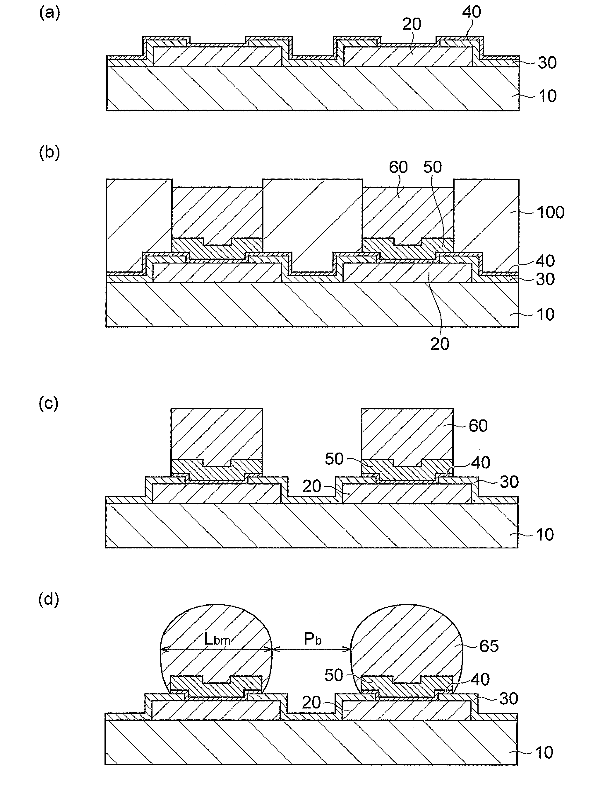
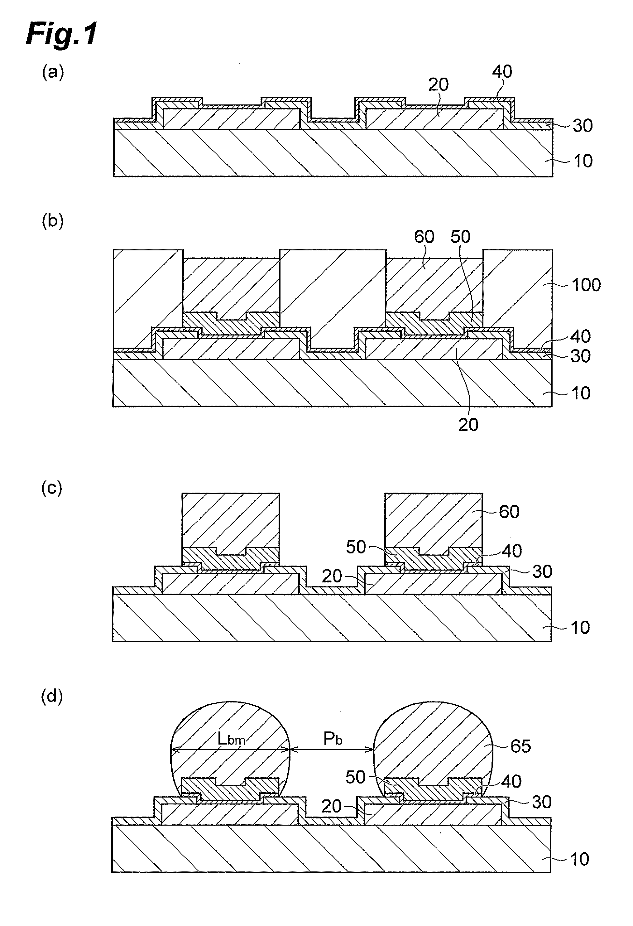
[0064](Substrate Preparation)

[0065]There was prepared a silicon substrate (5×5 mm, 0.6 mm thick) on which an external electrode and a SiN insulating coating layer having an opening are formed as illustrated in FIG. 2(a). Note that the external electrode was made of copper and the 10×10 openings were arranged so as to be equally spaced from each other. In addition, the silicon substrate was prepared such that the external electrode was pre-wired so as to form a daisy circuit at mounting in order to confirm conductivity at a heat cycle test to be described later.

[0066](Electroless Nickel Plating)

[0067]Then, predetermined pretreatments (degreasing, pickling, and activating treatments) were performed on a copper external electrode surface exposed in an opening of the SiN insulating coating layer, followed by electroless nickel plating, to form a UBM layer filling the opening and covering part of the SIN insulating coating layer (FIG. 2(b)). Note that as the electroless nickel plating, a...

examples 2 to 6

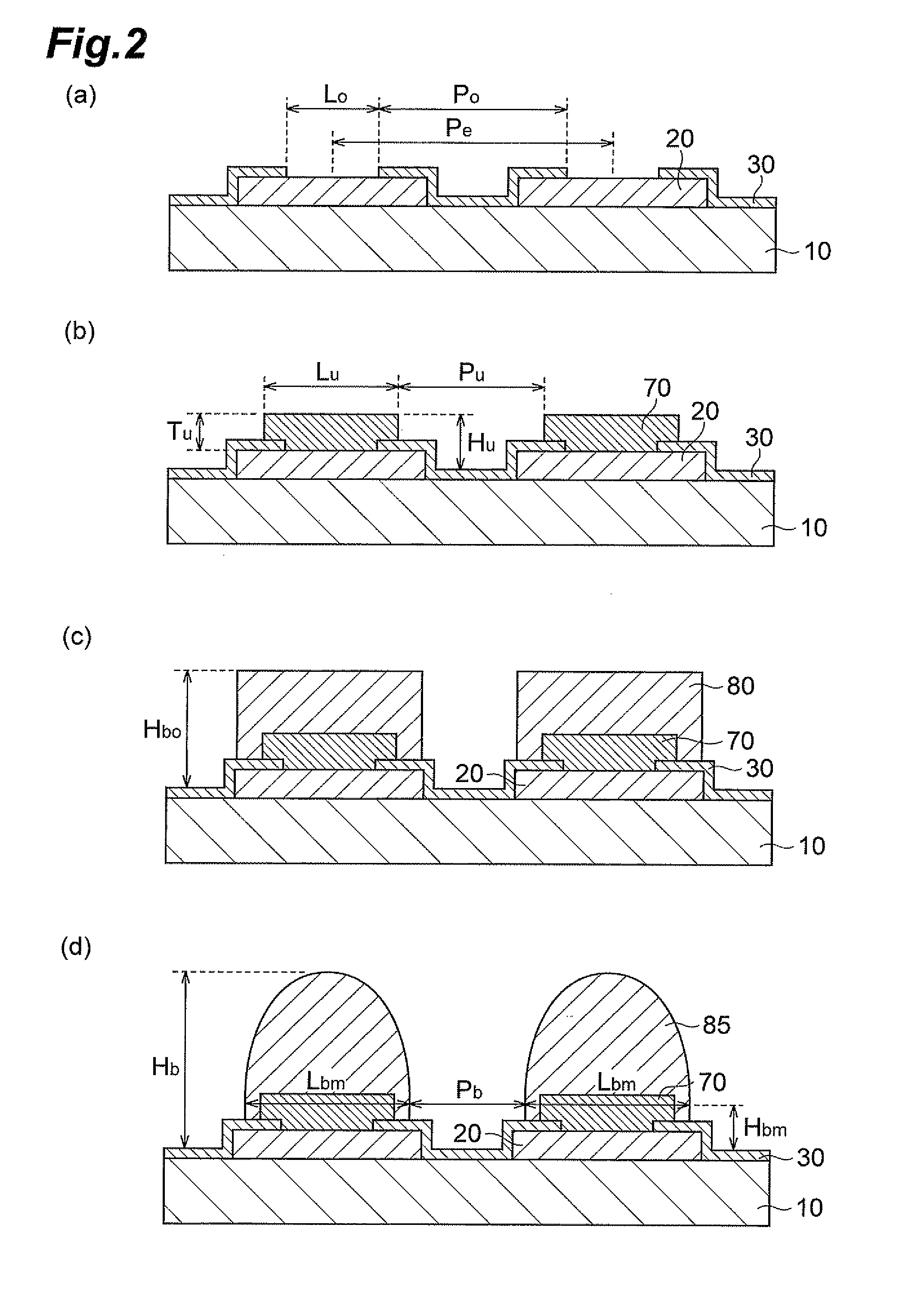
[0077]In the same manner as in example 1 except that the thickness, the pitch, and the like of each component were changed as shown in Table 1, there was obtained a silicon TEG substrate comprising a terminal structure as illustrated in FIG. 2(d).

example 7

[0078]In the same manner as in example 1 except that electrolytic nickel plating was performed instead of electroless nickel plating, there was obtained a silicon TEG substrate comprising a terminal structure as illustrated in FIG. 3(d).

[0079]The electrolytic nickel plating was performed in the following manner. First, a 0.1 μm thick copper layer was formed as a seed layer by sputtering on the copper external electrode surface exposed in the SiN insulating coating layer opening and the SiN insulating coating layer surface (FIG. 3(a)), and then a dry film was formed. Subsequently, the dry film was patterned by photoresist to remove the dry film around the SiN insulating coating layer opening. Then, electrolytic nickel plating was performed on the external electrode surface exposed in the SiN insulating coating layer opening and part of the insulating coating layer surface to form the UBM layer (FIG. 3(b)). Then, the dry film was stripped and an unnecessary seed layer was removed to f...


PUM


Abstract

The present invention relates to a terminal structure comprising: a base material 10; an external electrode 20 formed on the base material; an insulating coating layer 30 formed on the base material and on the electrode and having an opening exposing at least part of the electrode; an under-bump metal layer 70 filling the opening and covering part of the insulating coating layer; and a dome-shaped bump 85 covering the under-bump metal layer, wherein in a cross section along a lamination direction, a height Hbm at which the bump has a maximum diameter (Lbm) is lower than a maximum height Hu of the under-bump metal layer.

Description

BACKGROUND OF THE INVENTION[0001]1. Field of the Invention[0002]The present invention relates to a terminal structure and a semiconductor device.[0003]2. Related Background Art[0004]For high-density packaging of high performance semiconductors such as central processing unit (CPU), a transition is underway from a wire bonding mounting method as a general-purpose technique to a flip-chip mounting method of forming a bump made of solder or the like on a chip electrode and directly bonding the bump to a substrate.[0005]For example, Patent Literature 1 (Japanese Patent Laid-Open No. 2001-085456) and Patent Literature 2 (Japanese Patent Laid-Open No. 2002-203868) disclose methods of forming a bump on electrodes provided on a base material.SUMMARY OF TUE INVENTION[0006]With the miniaturization of semiconductor devices, it is needed to arrange bumps more closely to each other, that is, bump pitch reduction. Unfortunately, the use of the aforementioned conventional bumps cannot sufficiently...

Claims


Application Information

Patent Timeline
Patent Type & Authority Applications(United States)
IPC IPC(8): H01L23/00
CPCH01L24/13H01L24/03H01L24/05H01L24/11H01L2224/0345H01L2224/03462H01L2224/03464H01L2224/0347H01L2224/0401H01L2224/05022H01L2224/05572H01L2224/05655H01L2224/11464H01L2224/1147H01L2224/11849H01L2224/13005H01L2224/13006H01L2224/13023H01L2224/13111H01L2924/00014
Inventor YOSHIDA, KENICHIORIKASA, MAKOTOSEIKE, HIDEYUKIHORIKAWA, YUHEIABE, HISAYUKI
Owner TDK CORPARATION
Why Eureka
Try Eureka