Electrostatic discharge protection device

a protection device and electrostatic discharge technology, applied in semiconductor devices, semiconductor/solid-state device details, diodes, etc., can solve the problems of electrical overstress, damage or failure of integrated circuits in chips, easy damage to semiconductor and other circuit components in integrated circuits, etc., to save layout area, reduce and achieve the effect of reducing the distance between anodes

Active Publication Date: 2014-03-06
MACRONIX INT CO LTD
View PDF4 Cites 7 Cited by
  • Summary
  • Abstract
  • Description
  • Claims
  • Application Information

AI Technical Summary

Benefits of technology

[0008]This invention is also intended to provide an ESD protection device that allows reduction of the distance between the anode and the cathode to save the layout area, without adversely affecting the turn-on speed.
[0009]This invention is further intended to provide an ESD protection device in which the breakdown speed of the transistor can be adjusted by controlling the distance between the gate and a neighboring doped region.

Problems solved by technology

ESD means movement of electrostatic charges from a non-conductive surface, which easily damages the semiconductor and other circuit components in integrated circuits.
The transient power of the ESD will possibly cause damage or failure of the integrated circuits in the chip.
However, the holding voltage of the discharge path provided by such scheme is usually lower than 10.5 V, so that electrical overstress (EOS) events may occur frequently in operation of the internal circuits to disturb the same.

Method used


Image

  • Electrostatic discharge protection device
  • Electrostatic discharge protection device
  • Electrostatic discharge protection device

Examples


Embodiment Construction

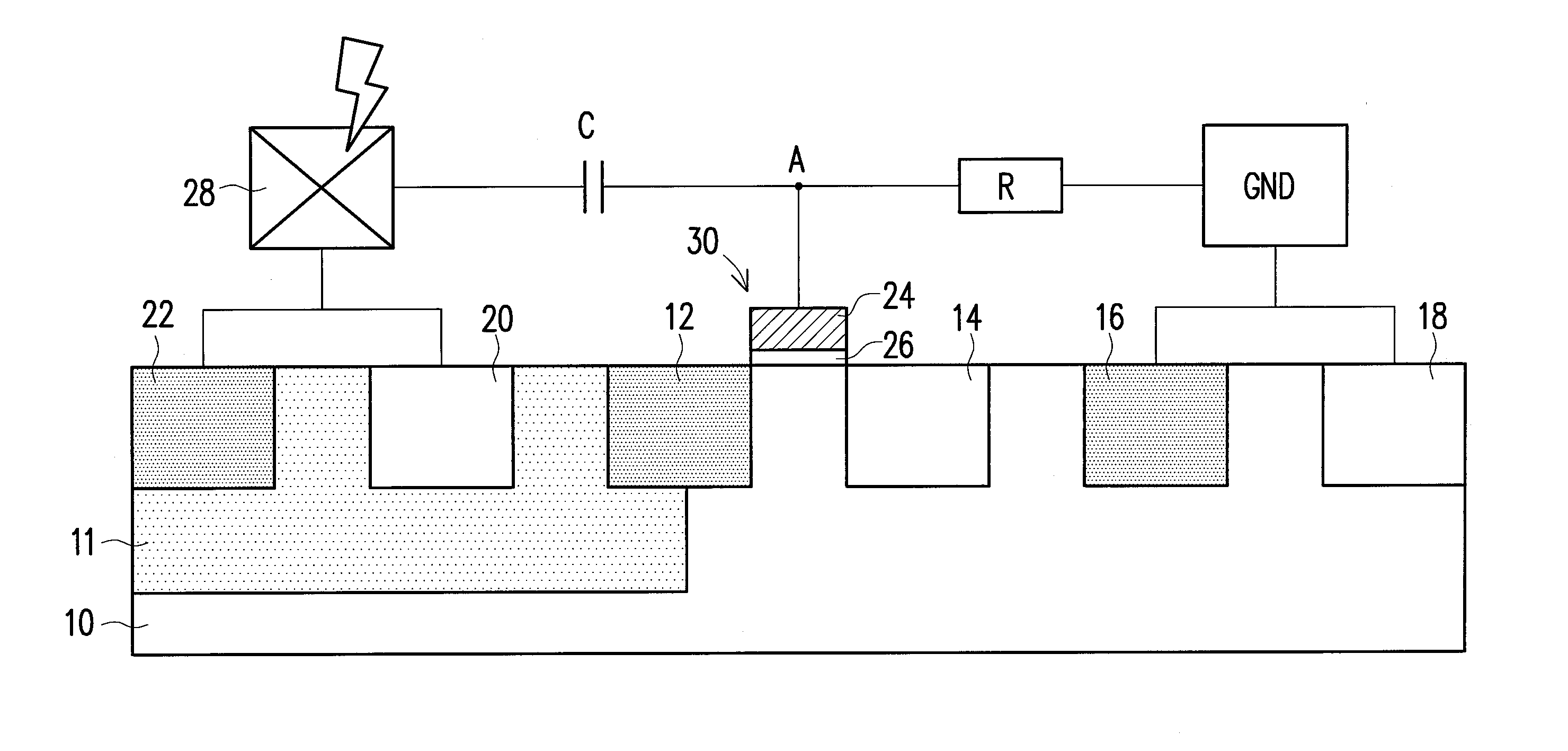
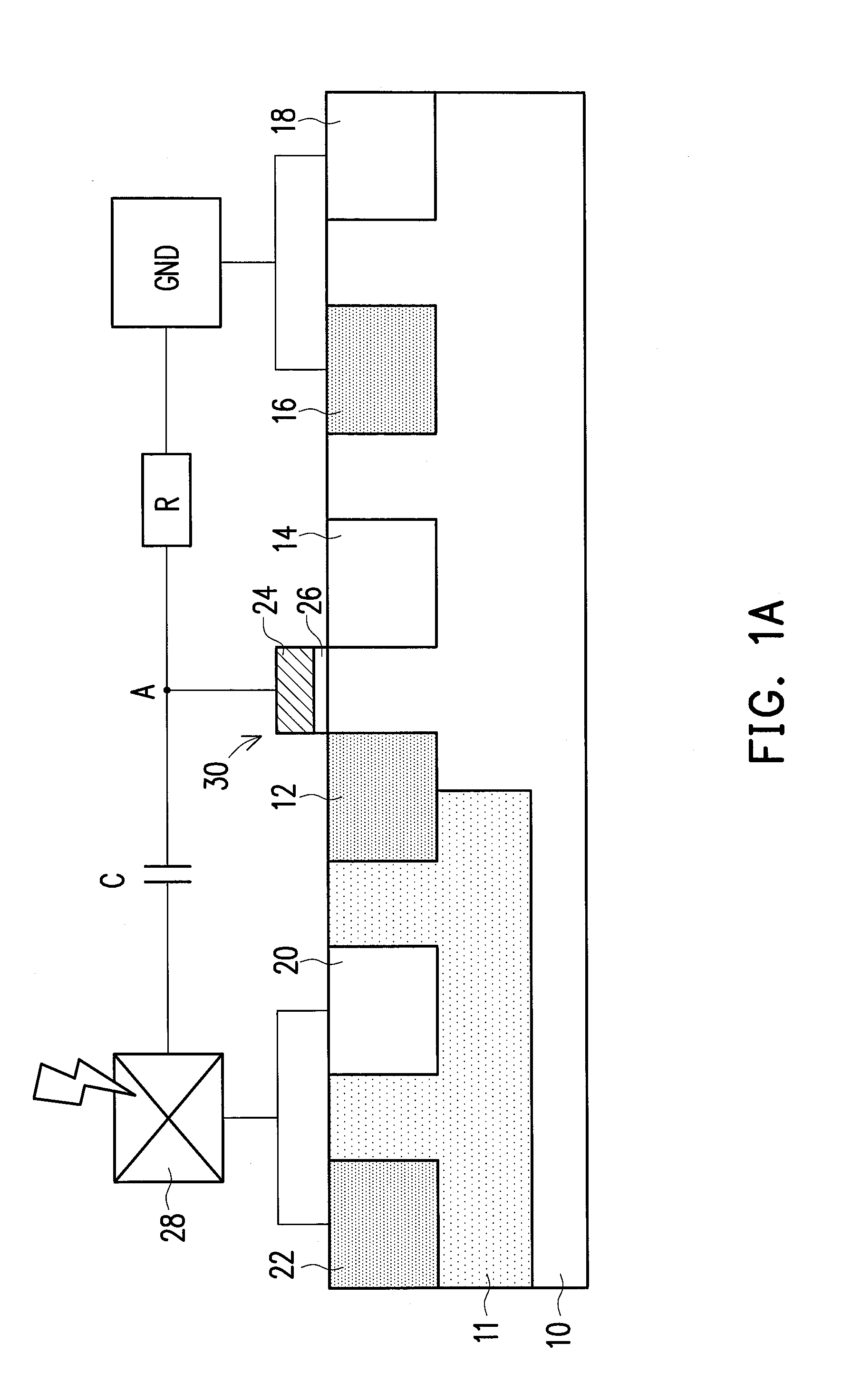
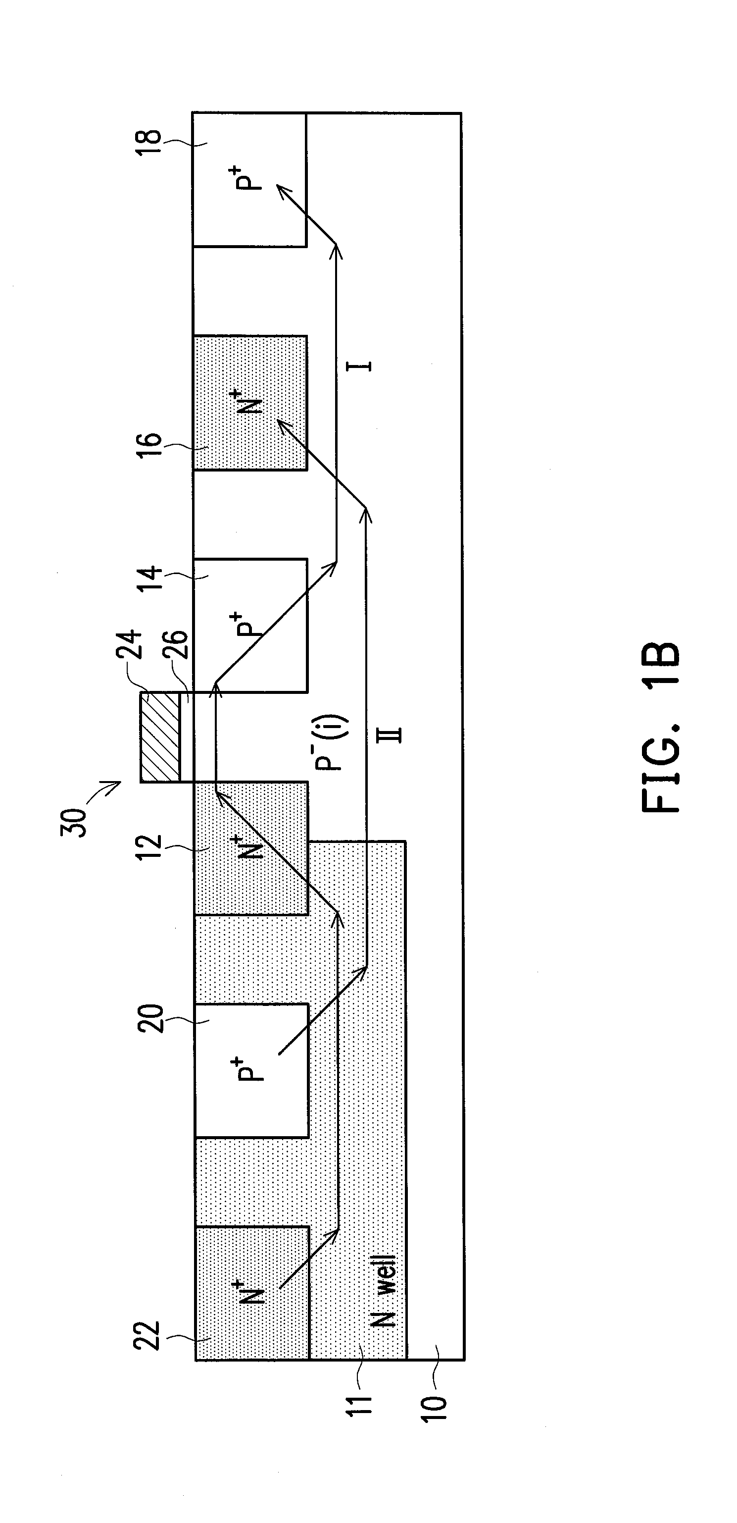
[0021]Referring to FIG. 1A, the ESD protection device includes a well 11 in a substrate 10, a plurality of doped regions (14, 18 and 20) of a first conductivity type, a plurality of doped regions (12, 16 and 22) of a second conductivity type, and a gate electrode 24 disposed over the substrate 10. More specifically, the ESD protection device includes a substrate 10, a well 11, a transistor 30 that includes a gate 24, a first doped region 12 and a second doped region 14, a third doped region 16, a fourth doped region 18, a fifth doped region 20 and a sixth doped region 22.

[0022]The well 11 is located in the substrate 10. The substrate 10 may be a single-element semiconductor substrate like a silicon substrate, or a semiconductor compound substrate. In an embodiment, the substrate 10 has a first conductivity type and the well 11 has a second conductivity type. In an embodiment, the first conductivity type is P-type and the second conductivity type is N-type. The P-type dopant may be b...


PUM


Abstract

An ESD protection device is described, including a substrate of a first conductivity, a well of a second conductivity, a transistor including a first doped region of the second conductivity located in the substrate and extending into the well, a second doped region of the first conductivity and a gate over the substrate between the two doped regions, a third doped region of the second conductivity and a fourth doped region of the first conductivity disposed in the substrate in sequence from an outer side of the second doped region and coupled to ground, and a fifth doped region of the first conductivity and a sixth doped region of the second conductivity disposed in the well in sequence from an outer side of the first doped region and coupled to a bonding pad. When an ESD voltage is applied to the bonding pad, it is coupled to the gate.

Description

BACKGROUND OF THE INVENTION[0001]1. Field of Invention[0002]This invention relates to an electrostatic discharge (ESD) protect circuit, and particularly to an ESD protect circuit of which the breakdown speed can be adjusted.[0003]2. Description of Related Art[0004]ESD means movement of electrostatic charges from a non-conductive surface, which easily damages the semiconductor and other circuit components in integrated circuits. For example, when an ordinary charged body, such as a human body walking on a carpet or a machine for packaging or testing integrated circuits, contacts a chip, it will discharge electricity to the chip. The transient power of the ESD will possibly cause damage or failure of the integrated circuits in the chip.[0005]To prevent damage of ICs by ESD, ESD protect circuits are usually included in an IC. There are various designs for ESD protect circuits, wherein an ordinary design includes two N-type transistors connected in series, of which the gate electrodes a...

Claims


Application Information

Patent Timeline
Patent Type & Authority Applications(United States)
IPC IPC(8): H01L29/06H01L27/06
CPCH01L27/0262H01L29/7436H01L29/87
Inventor HO, YUNG-HANG
Owner MACRONIX INT CO LTD
Why Eureka
Try Eureka