Antenna device and wireless device

a wireless device and antenna technology, applied in loop antennas, radiating element structure forms, instruments, etc., can solve the problems of increased insertion loss, complicated bonding process, and inability to ensure high connection reliability, so as to increase the maximum communication distance of rfid tags or readers/writers, the effect of low insertion loss

Active Publication Date: 2014-03-06
MURATA MFG CO LTD
View PDF3 Cites 23 Cited by
  • Summary
  • Abstract
  • Description
  • Claims
  • Application Information

AI Technical Summary

Benefits of technology

[0019]According to the antenna device of various preferred embodiments of the present invention, a coupling portion of an antenna element which is coupled to a feed element is disposed in a closed magnetic circuit constituted by coil conductors of the feed element and therefore the feed element and the antenna element can be coupled to each other more strongly. As a resul

Problems solved by technology

This type of bonding, however, uses ultrasonic waves and therefore the bonding process is complicated.
As a result, high connection reliability may not be ensured.
In an RFID tag in which a feed coil is connected to an RFIC chip and the feed coil is coupled to a main antenna via an electromagnetic field, connection between the RFIC chip and an antenna element can be readily made, however, this coupling is

Method used


Image

  • Antenna device and wireless device
  • Antenna device and wireless device
  • Antenna device and wireless device

Examples


first preferred embodiment

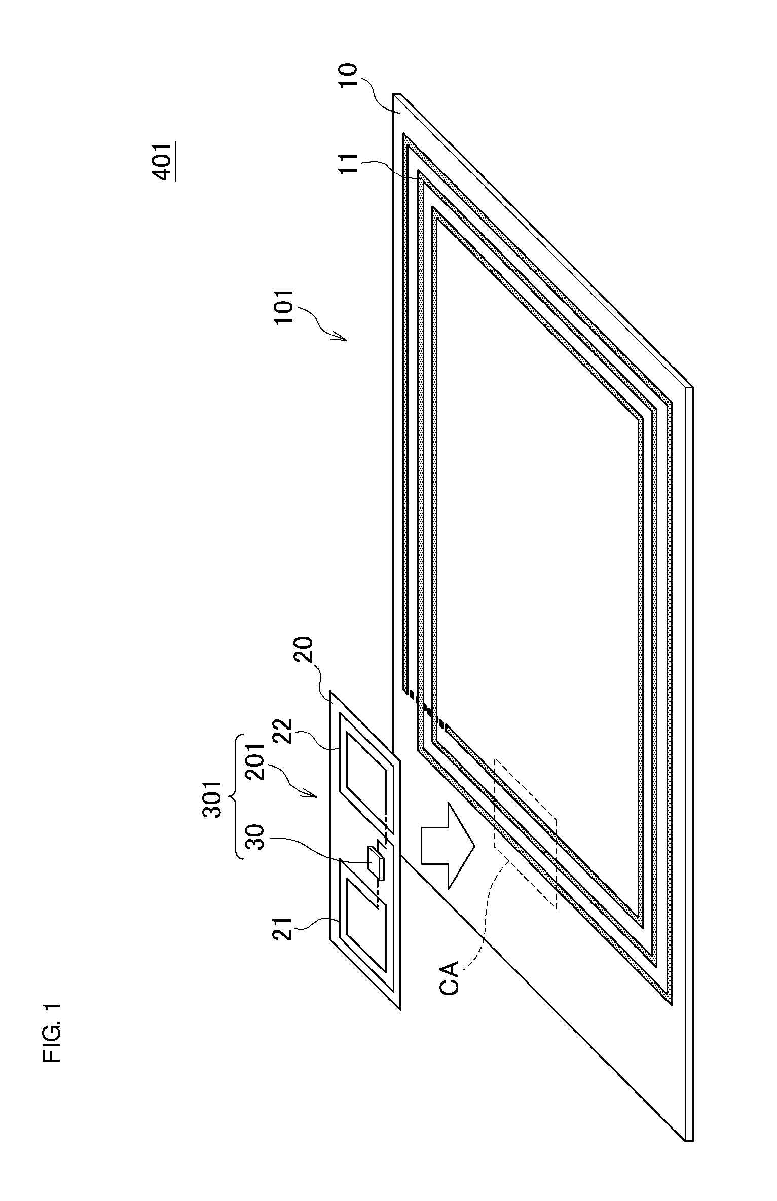
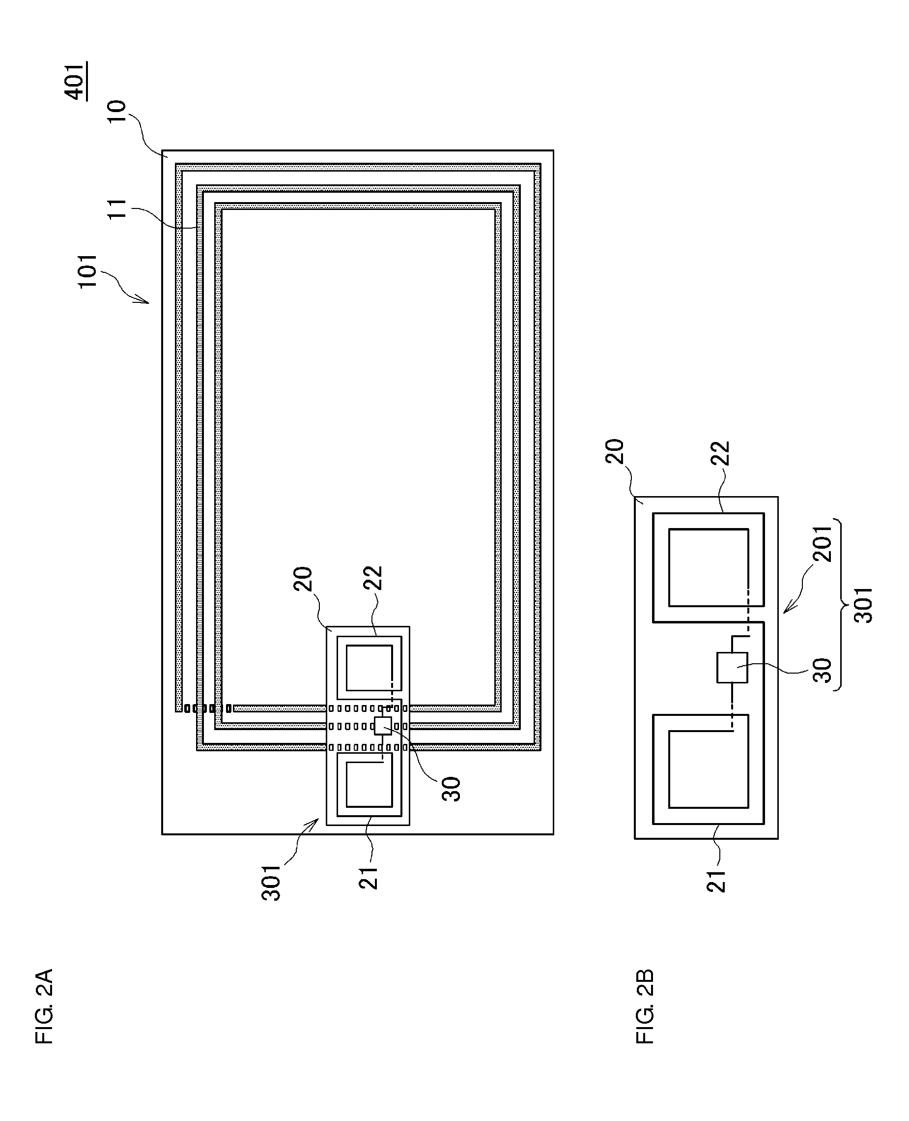
[0044]FIG. 1 is an exploded perspective view of an RFID tag 401 according to a first preferred embodiment of the present invention. FIG. 2A is a plan view of the RFID tag 401, and FIG. 2B is a plan view of a feed device 301.

[0045]In this example, the RFID tag 401 is an RFID tag for an HF-band RFID system and includes an antenna element 101 and the feed device 301. The antenna element 101 preferably includes a base sheet 10 made of PET or the like and a coil conductor 11 located on the upper surface thereof. The feed device 301 preferably includes a feed element 201 and an RFIC 30.

[0046]The RFIC 30 is an IC chip for RFID. The RFIC 30 preferably includes a memory circuit, a logic circuit, and the like.

[0047]The feed element 201 preferably includes a base sheet 20 made of PET or the like, and a first coil conductor 21 and a second coil conductor 22 located on the upper surface of the base sheet 20.

[0048]As described below in detail, the first coil conductor and the second coil conducto...

second preferred embodiment

[0057]In a second preferred embodiment of the present invention, a structure of an antenna element which is different from that in the first preferred embodiment is described.

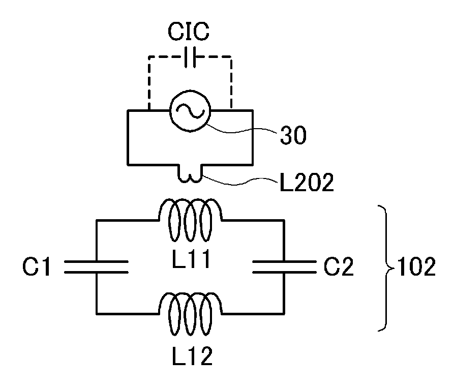
[0058]FIG. 4A is an exploded perspective view of coil conductors 11 and 12 included in an antenna element 102. The coil conductor 11 is located on a first main surface of a base sheet (not illustrated in FIG. 4) and the coil conductor 12 is located on a second main surface of the base sheet.

[0059]FIG. 4B is an equivalent circuit diagram of the antenna element 102 illustrating the case where the two coil conductors 11 and 12 face each other with the base sheet interposed therebetween. FIG. 4C is an equivalent circuit diagram illustrating the case where the feed device is coupled to the antenna element.

[0060]As illustrated in FIG. 4A, the coil conductor 11 and the coil conductor 12 of the antenna element 102 are preferably arranged in a rectangular or substantially rectangular spiral pattern. The winding directio...

third preferred embodiment

[0062]In a third preferred embodiment of the present invention, a structure of a feed element and a feed device, which is different from that in the first preferred embodiment, is described.

[0063]FIG. 5 is an exploded perspective view of a feed element 203 and a feed device 303 according to the third preferred embodiment. The feed element 203 includes a plurality of stacked dielectric base sheets on each of which a pattern of a coil conductor or the like is provided. Terminals 23 and 24 to connect the RFIC 30 are provided on a base sheet 20a. Coil conductors 21b and 22b are provided on a base sheet 20b. Coil conductors 21c and 22c are provided on a base sheet 20c. Coil conductors 21d and 22d are provided on a base sheet 20d. Via conductors are provided on each of the base sheets as shown by the dashed lines in FIG. 5 to define inter-layer connections.

[0064]The coil conductors 21b, 21c, and 21d and the via conductors connecting these coil conductors constitute the first coil conducto...


PUM


Abstract

An RFID tag includes an antenna element and a feed device. The antenna element includes a base sheet and a coil conductor on the upper surface thereof. The feed device includes a feed element and an RFIC. The feed element includes a base sheet and a first coil conductor and a second coil conductor on the upper surface of the base sheet. The first coil conductor and the second coil conductor are arranged on the base sheet such that magnetic flux generated in the first coil conductor and the second coil conductor constitutes a closed magnetic circuit. The feed device is adhered to a coupling portion of the antenna element. As a result, the RFIC is strongly coupled to the antenna element.

Description

BACKGROUND OF THE INVENTION[0001]1. Field of the Invention[0002]The present invention relates to an antenna device and a wireless device including the same.[0003]2. Description of the Related Art[0004]The radio frequency identification (RFID) system, in which a reader / writer and an RFID tag communicate with each other in a non-contact manner to transmit information between the reader / writer and the RFID tag, has become widespread. Such an RFID tag and a reader / writer include a radio frequency integrated circuit (RFIC) chip that processes high frequency signals and an antenna element that emits or receives high frequency signals. Examples of known RFID systems include the HF-band RFID system using the 13 MHz band, such as FeliCa®, and the UHF-band RFID system using the 900 MHz band which is used in warehouse management and the like.[0005]A general RFID tag often adopts bonding that uses a gold bump for connecting an RFIC chip to an antenna element. This type of bonding, however, uses...

Claims


Application Information

Patent Timeline
IPC IPC(8): H01Q1/50H01Q7/00
CPCH01Q7/00H01Q1/50H01Q1/2225G06K19/07794H01Q1/38
Inventor KATO, NOBORU
Owner MURATA MFG CO LTD
Why Eureka
Try Eureka