Thin film sensor, capacitive touch panel having the same and preparation method thereof and terminal product

a capacitive touch panel and sensor technology, applied in capacitor manufacture, variable capacitors, instruments, etc., can solve the problems of high cost, complicated fabrication process, and increased consumption of raw materials, and achieve the effect of thin film sensors

Inactive Publication Date: 2014-03-13
SHENZHEN O FILM TECH
View PDF9 Cites 9 Cited by
  • Summary
  • Abstract
  • Description
  • Claims
  • Application Information

AI Technical Summary

Benefits of technology

[0008]The obtained thin film sensor used in the capacitive touch panel has only one optical conductive substrate, specifically, it has only one optically transparent substrate, two surfaces of the substrate are coated with the sensing electrode layer and driving electrode layer respectively, which, on one hand, helps to reduce the thickness of the thin film sensor, thus contributes to the development of light and thin of a touch panel and touch electronics; on the other hand, the material selection and the preparation process are very simple, the selection of two substrates is not necessary to prepare the two optically transparent thin films.
[0016]According to one embodiment, the optical glue is an optical clear adhesive (OCA) with the thickness of 50 micrometers to 100 micrometers. In a preferred embodiment, the transmittance of the optical glue is more than 95%, which ensures the durability of the adhesive, the color and the sufficient display brightness.

Problems solved by technology

The conventional thin film touch sensor is too thick, which would increase the thickness of the touch panel and do not contribute to the development of light and thin of the touch panel and touch electronics; and the raw materials are consumed more, the cost is high, the fabrication process is complicated.

Method used


Image

  • Thin film sensor, capacitive touch panel having the same and preparation method thereof and terminal product
  • Thin film sensor, capacitive touch panel having the same and preparation method thereof and terminal product
  • Thin film sensor, capacitive touch panel having the same and preparation method thereof and terminal product

Examples


Embodiment Construction

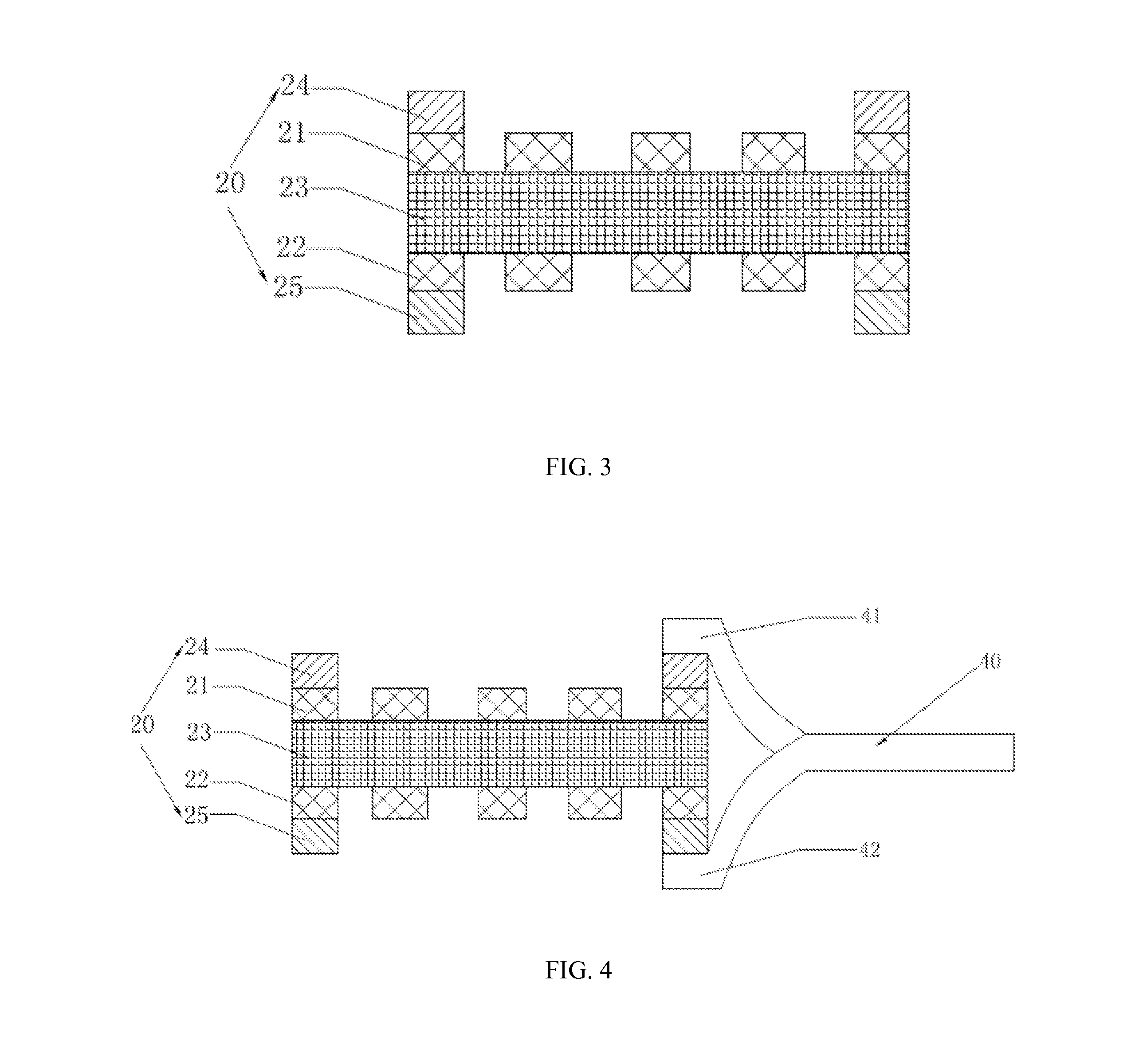
[0034]FIG. 6 is a cross-section view of the capacitive touch panel in accordance with the first embodiment; the capacitive touch panel includes a cover lens 10 and a thin film sensor 20.

[0035]The cover lens 10 is made of an irregular shaped toughened glass.

[0036]The cover lens 10 is provided with a window frame 11 on a lower surface (a surface which is bonded to the thin film sensor) thereof, generally speaking, the window frame 11 is set on the cover lens 10 by screen printing technique with all kinds of colour inks

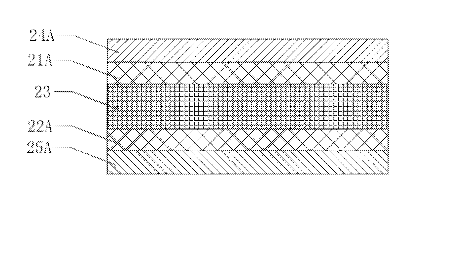
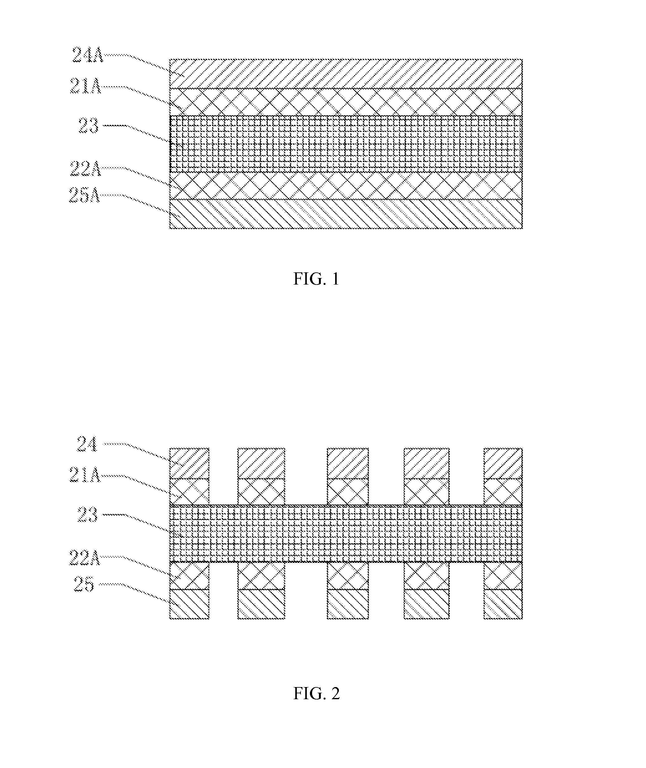
[0037]The thin film sensor 20 includes a sensing electrode layer 21, a driving electrode layer 22, and a substrate 23.

[0038]The substrate 23 is a single layer PET film, which is substantially optically transparent.

[0039]The substrate 23 has an upper surface and a lower surface, the sensing electrode layer 21 and the driving electrode layer 22 are coated on the upper and lower surfaces, respectively, the sensing electrode layer 21 is closer to the cover lens 10 compared t...


PUM

PropertyMeasurementUnit
thicknessaaaaaaaaaa
thicknessaaaaaaaaaa
transmittanceaaaaaaaaaa

Abstract

The present invention relates to a thin film sensor, capacitive touch panel having the sensor and preparation method thereof and terminal product. The thin film sensor of the present invention has only one optically conductive substrate. Specifically, only one optically transparent substrate is used, a sensing electrode layer and a driving electrode layer are coated on the upper and lower surfaces of the substrate, respectively, which helps to reduce the thickness of the thin film sensor on one hand, thus contributes to the development of light and thin of a touch panel and touch electronics; on the other hand, the material selection and the preparation process are simple, the selection of two substrates is not necessary to prepare two optically conductive thin film.

Description

FIELD OF THE INVENTION[0001]The present invention relates to the thin film sensor, capacitive touch panel having the sensor and preparation method thereof and terminal product.BACKGROUND OF THE INVENTION[0002]Currently, the touch intelligent electronic devices are very popular in the market, the capacitive touch panel has been widely recognized due to its good Human-Machine interaction.[0003]Generally speaking, capacitive touch panels can be divided into both the glass capacitive screen and thin film capacitive screen according to the substrate material of the sensor. The thin film capacitive touch panels are widely used in the smart phone, tablet computer and ultrabook due to that its sensor is lighter than the sensor of the glass capacitive touch panel, and the thin film material can be produced by the roll to roll manner which is conductive to mass production and enables lower production cost. The thin film capacitive touch panel has nearly the same size of market with the glass ...

Claims


Application Information

Patent Timeline
Patent Type & Authority Applications(United States)
IPC IPC(8): G01R27/26H01G5/18
CPCH01G5/18G01R27/2605G06F2203/04103G06F3/0445
Inventor CHENG, ZHIZHENGMENG, KAITANG, GENCHU
Owner SHENZHEN O FILM TECH
Why Eureka
Try Eureka