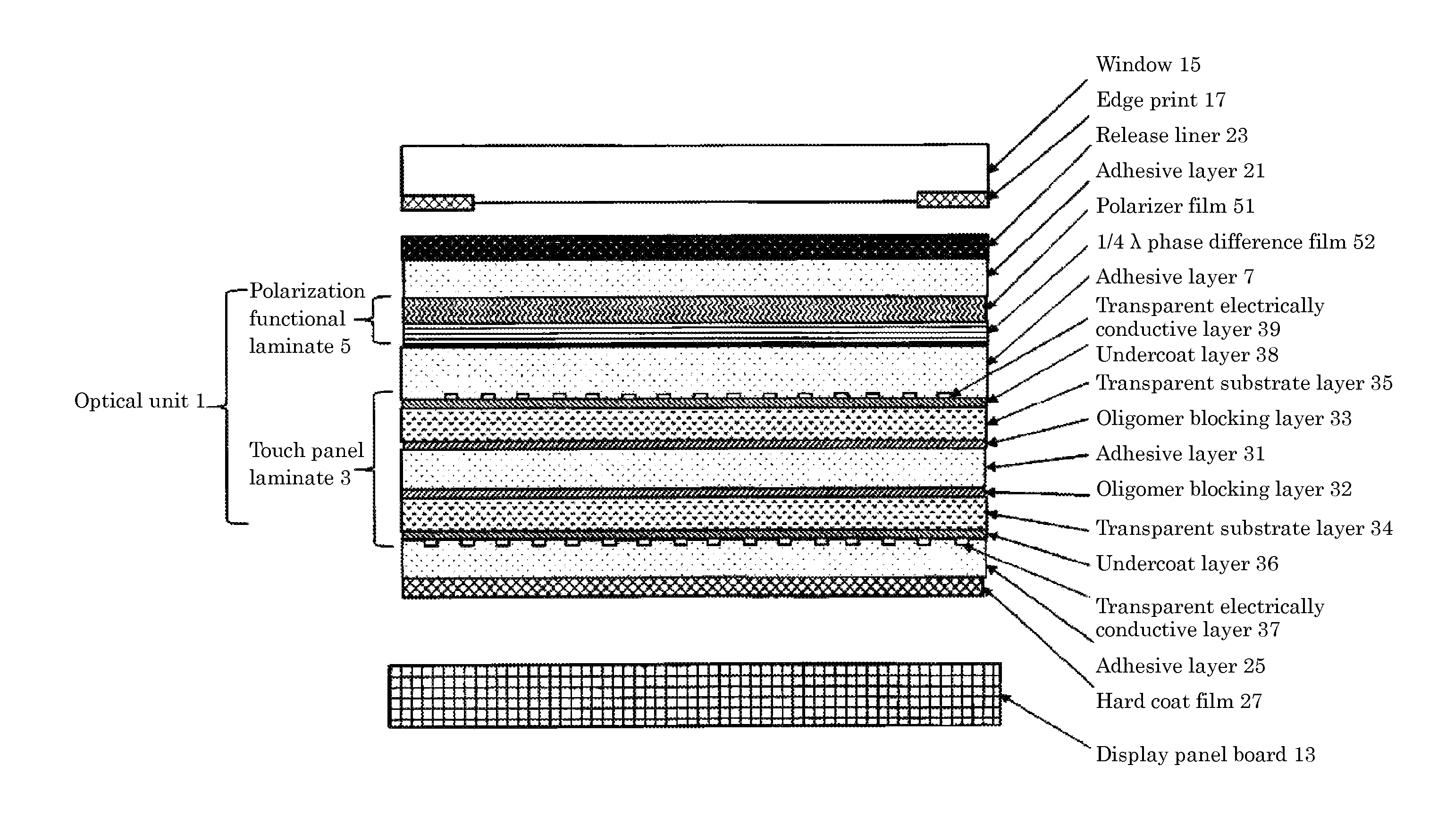
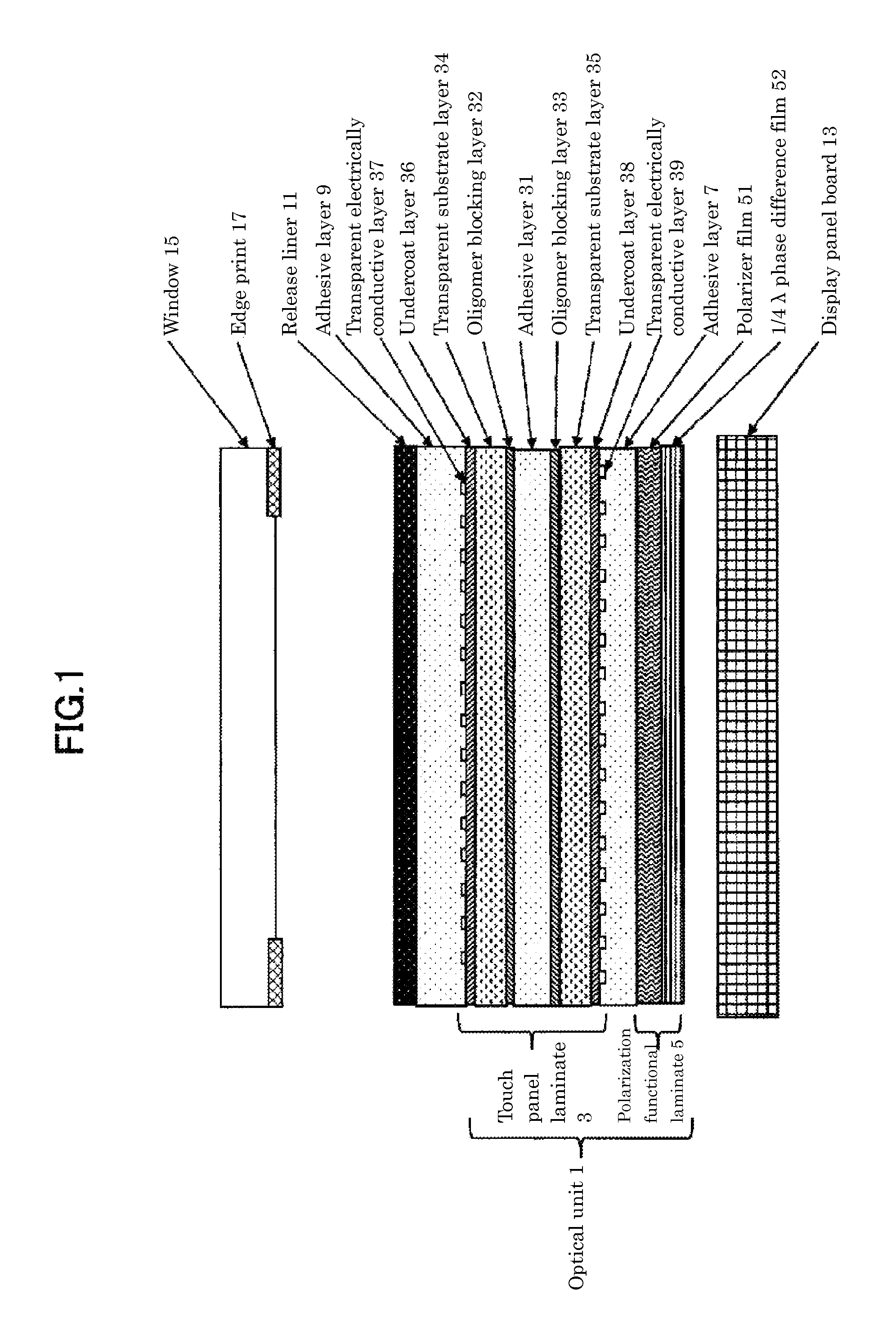
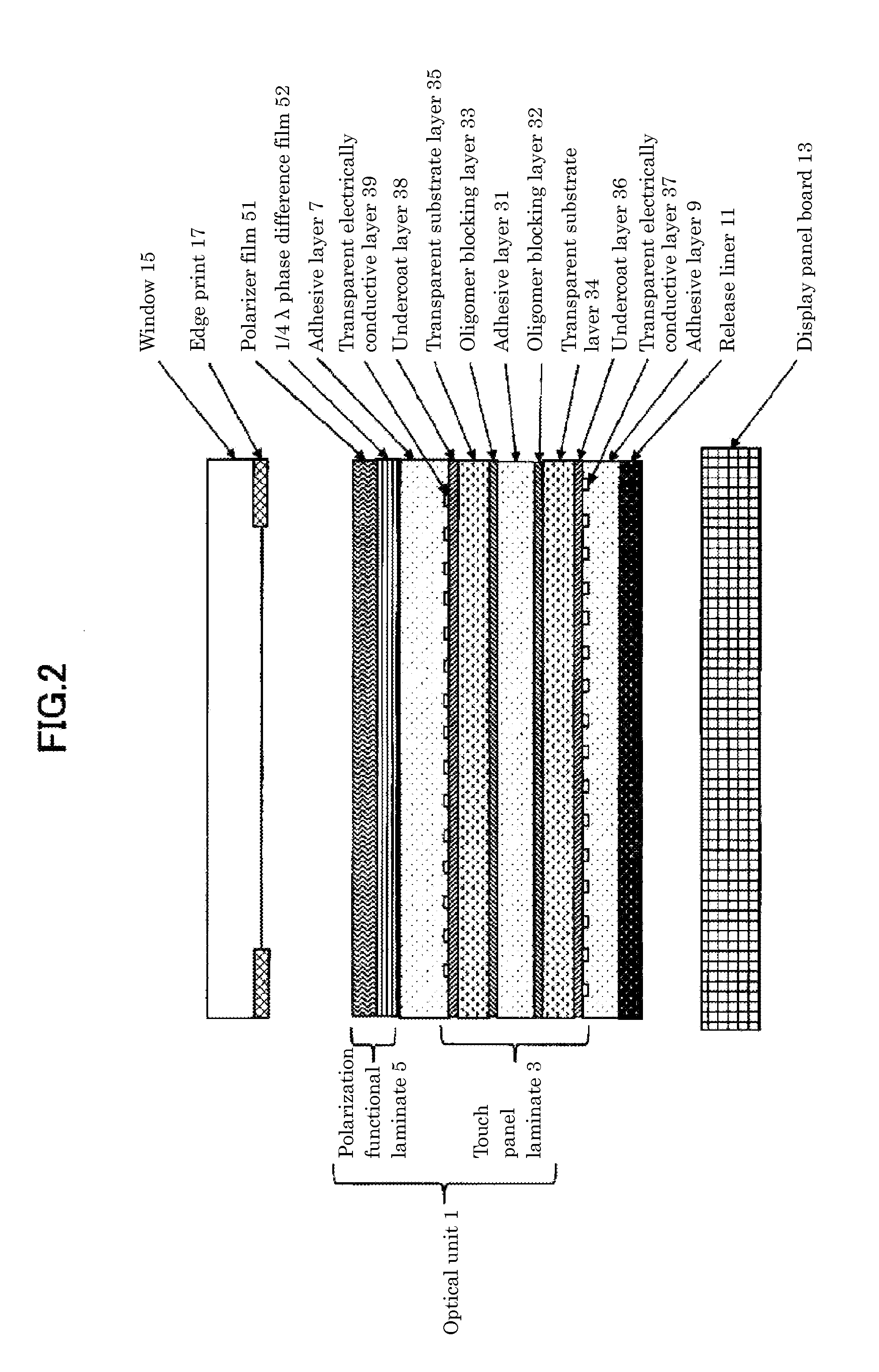
Display panel device with touch input function, optical unit for said display panel device, and production method for same
- Summary
- Abstract
- Description
- Claims
- Application Information
AI Technical Summary
Benefits of technology
Problems solved by technology
Method used
Image

Examples
example 1
[0067](Formation of Optically Transparent Adhesive Layer)
[0068]FIG. 5 is a process diagram illustrating a process of producing an optically transparent adhesive layer usable in the present invention. First of all, a monomer as a basic raw material of an adhesive and a polymerization initiator were mixed and stirred together with a solvent. As the monomer, a mixture consisting of 70 weight parts of 2-methoxyethyl acrylate, 29 weight parts of 2-ethylhexyl acrylate, and 1 weight parts of 4-hydroxybutyl acrylate was used. 0.2 weight parts of 2, 2′-azobisisobutyronitrile was used as the polymerization initiator, and 100 weight parts of ethyl acetate was used as a polymerization solvent. These materials were put in a separable flask, and stirred for one hour while introducing nitrogen gas thereinto (S5-1). After removing oxygen in a polymerization system in the above manner, the solution was heated up to 63° C. to conduct a reaction for 10 hours (S5-2), and then toluene was added to obtai...
PUM
| Property | Measurement | Unit |
|---|---|---|
| Electrical conductivity | aaaaa | aaaaa |
| Length | aaaaa | aaaaa |
| Shape | aaaaa | aaaaa |
Abstract
Description
Claims
Application Information
 - Generate Ideas
- Intellectual Property
- Life Sciences
- Materials
- Tech Scout
- Unparalleled Data Quality
- Higher Quality Content
- 60% Fewer Hallucinations
Browse by: Latest US Patents, China's latest patents, Technical Efficacy Thesaurus, Application Domain, Technology Topic, Popular Technical Reports.
© 2025 PatSnap. All rights reserved.Legal|Privacy policy|Modern Slavery Act Transparency Statement|Sitemap|About US| Contact US: help@patsnap.com