Method of fabricating a semiconductor package

a technology of semiconductor packaging and packaging, which is applied in the direction of semiconductor devices, semiconductor/solid-state device details, electrical equipment, etc., can solve the problems of reducing affecting the product yield of the overall package, and wasting time in the fabrication process. achieve the effect of reducing fabrication cost, preventing warpage of the overall structure, and increasing product yield

Inactive Publication Date: 2014-03-13
SILICONWARE PRECISION IND CO LTD
View PDF6 Cites 18 Cited by
  • Summary
  • Abstract
  • Description
  • Claims
  • Application Information

AI Technical Summary

Benefits of technology

[0011]Therefore, by keeping the first carrier flat and free of warpage, the present invention prevents warpage of the overall structure. Compared with the prior art, the present invention makes it possible for a testing process to be performed earlier to determine the electrical contact quality of the substrate, thereby increasing product yield and reducing fabrication cost. Further, instead of the conventional molding, the present invention forms an underfill between the first semiconductor chip and the first surface of the substrate to reduce fabrication cost and facilitate a multi-layer stack packaging of a plurality of semiconductor chips. Furthermore, since most surfaces of the semiconductor chips are exposed without the underfill covering, thus thermal dissipation effect is improved.
[0012]In addition, metal, dielectrics, and their associated geometric distributions in the substrate can be optimized or adjusted to match the upper first semiconductor chip and the lower packaging substrate in effective coefficient of thermal expansion (CTE), thereby alleviating warpage of the semiconductor package, increasing product yield, improving thermal dissipation and increasing product reliability.

Problems solved by technology

However, as such a TSI module is integrated with more semiconductor chips and its TSI becomes thinner, the ratio of metal to silicon in the TSI increases, thereby easily causing warpage and adversely affecting the product yield of the overall package.
Although the above-described package has a reduced thickness compared with the conventional packages, the fabrication process of the package is time-consuming Further, when the silicon wafer is thinned, the TSVs of the silicon wafer can be easily damaged.
The damaged TSVs cannot be easily tested since the fabrication of the TSVs is not actually finished until conductive bumps are formed on the lower side of the silicon wafer.
Furthermore, the silicon wafer is easy to warp during the fabrication process, thus reducing product yield and increasing fabrication cost.
Moreover, the molding compound adversely affects thermal dissipation of the package.

Method used


Image

  • Method of fabricating a semiconductor package
  • Method of fabricating a semiconductor package
  • Method of fabricating a semiconductor package

Examples


Embodiment Construction

[0014]The following embodiments are provided to illustrate the disclosure of the present invention, these and other advantages and effects can be apparent to those in the art after reading this specification.

[0015]It should be noted that all the drawings are not intended to limit the present invention. Various modification and variations can be made without departing from the spirit of the present invention. Further, terms, such as “upper”, “lower”, “warpage-free”, “flat”, “attach”, “a” etc., are merely for illustrative purpose and should not be construed to limit the scope of the present invention.

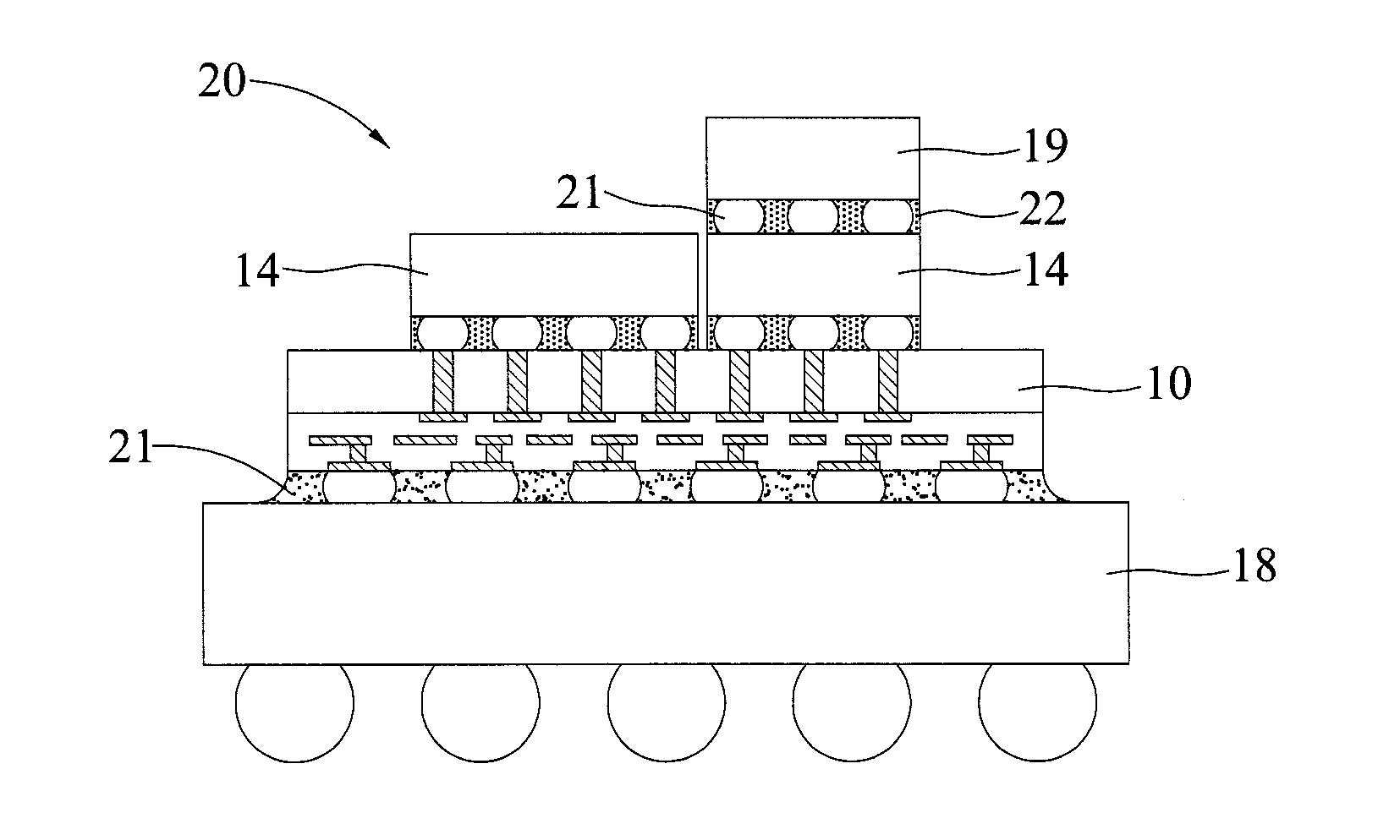
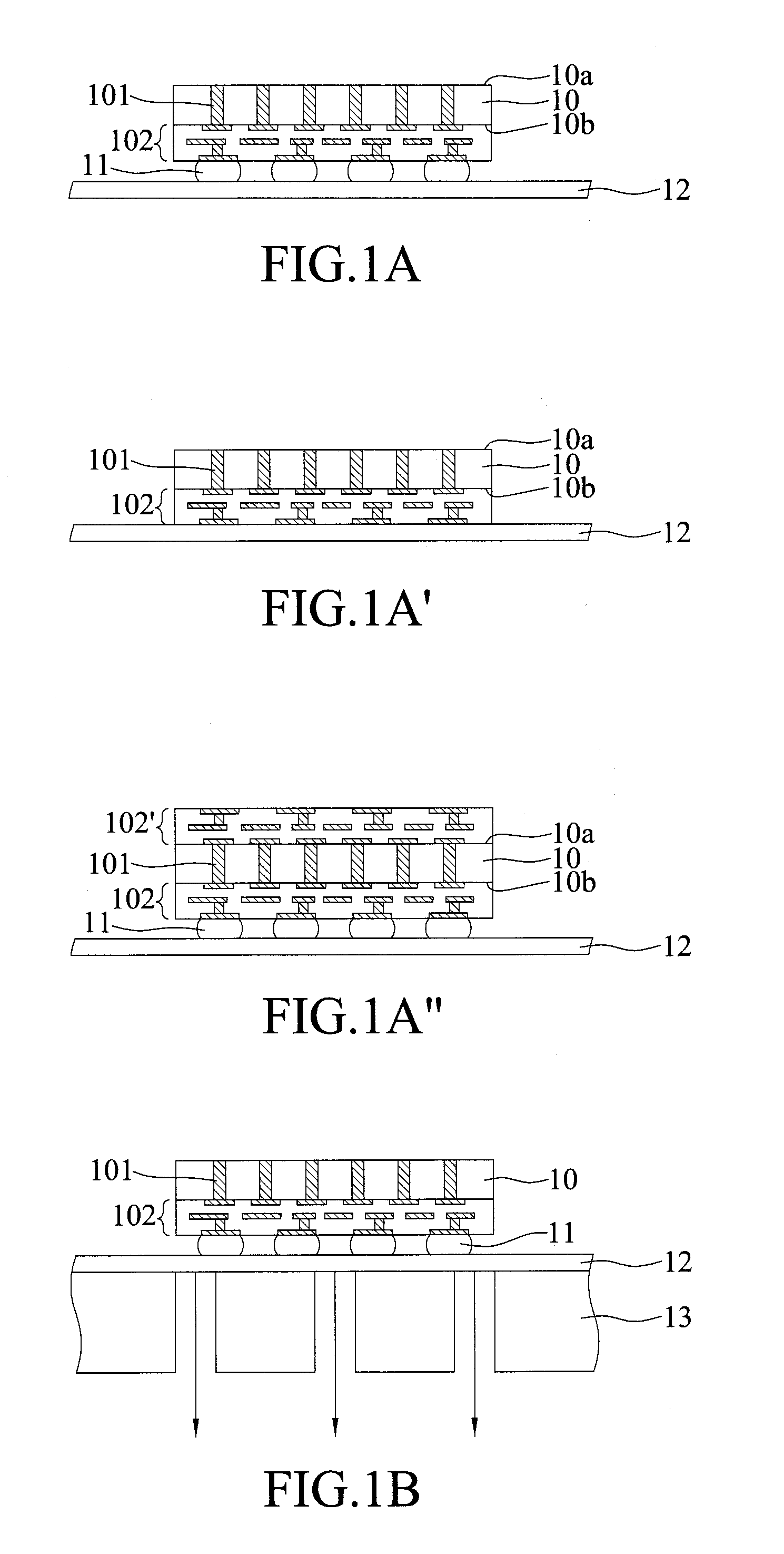
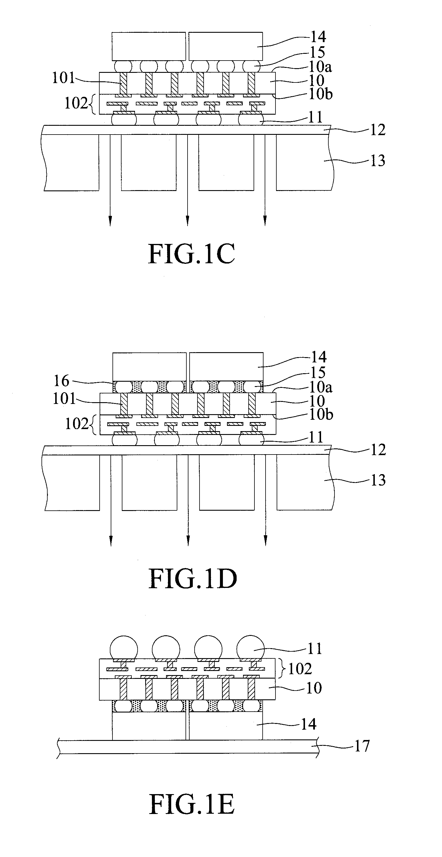
[0016]FIGS. 1A to 1F-4 are cross-sectional views illustrating a semiconductor package and a method of fabricating the semiconductor package according to the present invention. FIGS. 1A′ and 1A″ show different embodiments of FIG. 1A, and FIGS. 1F-2, 1F-3 and 1F-4 show different embodiments of FIG. 1F-1.

[0017]Referring to FIG. 1A, a substrate 10 is provided. The substrate 10 has opposite fi...


PUM


Abstract

A method of fabricating a semiconductor package is provided, including: providing a substrate having opposite first and second surfaces and a plurality of conductive through holes penetrating the first and second surfaces, disposing the substrate on a first carrier through the second surface thereof, and keeping the first carrier flat and free of warpage; attaching at least a first semiconductor chip to the first surface of the substrate and electrically connecting the first semiconductor chip and the substrate; removing the first carrier; and attaching the substrate to a packaging substrate through the second surface thereof and electrically connecting the substrate and the packaging substrate, thereby preventing the semiconductor package from warpage, increasing product yield, reducing fabrication cost, and improving thermal dissipation.

Description

BACKGROUND OF THE INVENTION[0001]1. Field of the Invention[0002]The present invention relates to methods of fabricating semiconductor packages, and, more particularly, to a method of fabricating a semiconductor package having an interposer.[0003]2. Description of Related Art[0004]To meet the trend of miniaturization, multi-function, high electrical performance and high operational speed of electronic products, nowadays semiconductor packaging industry follows this trend to develop packages with the characteristics of miniaturization, superior electrical performance, multi-function, and high speed.[0005]Flip-chip technology can be applied to reducing chip packaging sizes and shortening signal transmission paths and therefore has become widely used in semiconductor chip packaging. Various packages types, such as chip scale packages (CSPs), direct chip attached (DCA) packages and multi-chip module (MCM) packages, have been achieved by the flip-chip method.[0006]Further, TSI (through si...

Claims


Application Information

Patent Timeline
Patent Type & Authority Applications(United States)
IPC IPC(8): H01L21/56
CPCH01L21/56H01L21/563H01L2224/32225H01L2224/32145H01L2224/16225H01L2224/16145H01L2224/73204H01L2924/3511H01L2924/15311H01L2224/83005H01L2924/141H01L24/13H01L24/14H01L24/16H01L24/29H01L21/6836H01L24/73H01L24/81H01L24/83H01L24/92H01L25/0652H01L25/0655H01L2224/131H01L2224/14181H01L2224/16235H01L2224/2929H01L2224/29387H01L2224/81005H01L2224/92125H01L2225/06517H01L2924/1421H01L2924/1431H01L2924/1434H01L2225/06513H01L23/49816H01L23/49827H01L21/486H01L25/0657H01L25/50H01L2224/17181H01L2924/00012H01L2924/00H01L2924/014
Inventor HUANG, PIN-CHENGLAI, YI-CHE
Owner SILICONWARE PRECISION IND CO LTD
Why Eureka
Try Eureka