Quantum dot array devices with metal source and drain

a quantum dot array and metal source technology, applied in the direction of transistors, semiconductor devices, electrical apparatus, etc., can solve the problems of strained silicon and other new technologies failing to address all of the technology challenges, and unable to maintain precise control of various electrical characteristics of bulk semiconductor devices, etc., to achieve precise control of the conductive properties of crystalline materials

Active Publication Date: 2014-03-27
STMICROELECTRONICS INT NV
View PDF58 Cites 23 Cited by
  • Summary
  • Abstract
  • Description
  • Claims
  • Application Information

AI Technical Summary

Benefits of technology

[0008]Quantum dots are materials (e.g., semiconductors, metals) whose electronic characteristics are closely related to their crystal structure. Quantum dot structures have intermediate electronic properties that differ from both bulk materials and discrete molecules, and these electronic properties can be tuned by varying the size and spacing of the quantum dot crystals. Thus, quantum dots allow more precise control over conductive properties of the crystalline materials by altering the fundamental crystalline structure. Changes in the crystalline structure in turn influence the energy band structure and, specifically, the energy band gap of the semiconductor crystal. The embodiments discussed herein incorporate metallic quantum dots into the source and drain regions of a MOSFET to assist in controlling the transistor performance. In a first embodiment, metal quantum dots are incorporated into ion-doped source and drain regions; in a second embodiment, metal quantum dots are incorporated into in-situ-doped epitaxial source and drain regions.

Problems solved by technology

As technology nodes for integrated circuits scale below 10 nm, maintaining precise control of various electrical characteristics in bulk semiconductor devices becomes increasingly more challenging.
However, strained silicon and other new technologies fail to address all of the technology challenges listed above.

Method used


Image

  • Quantum dot array devices with metal source and drain
  • Quantum dot array devices with metal source and drain
  • Quantum dot array devices with metal source and drain

Examples


first embodiment

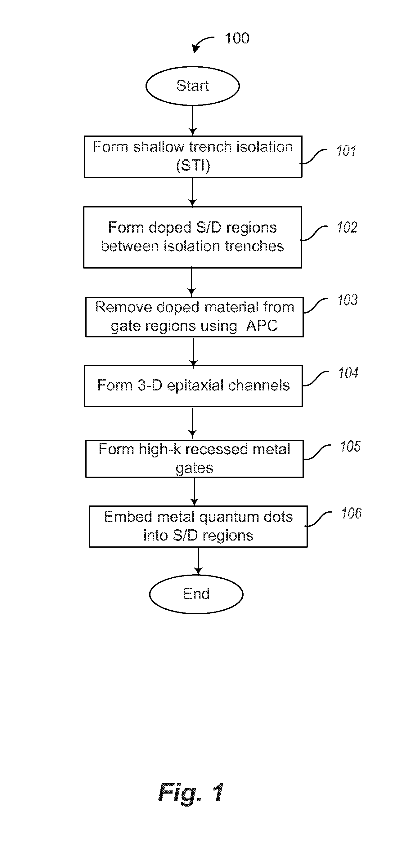
[0051]FIG. 1 shows a high-level sequence of processing steps in a method 100 that can be used to create a metal quantum dot array device, according to a The device described herein incorporates metal quantum dots into the source and drain regions of a MOSFET transistor.

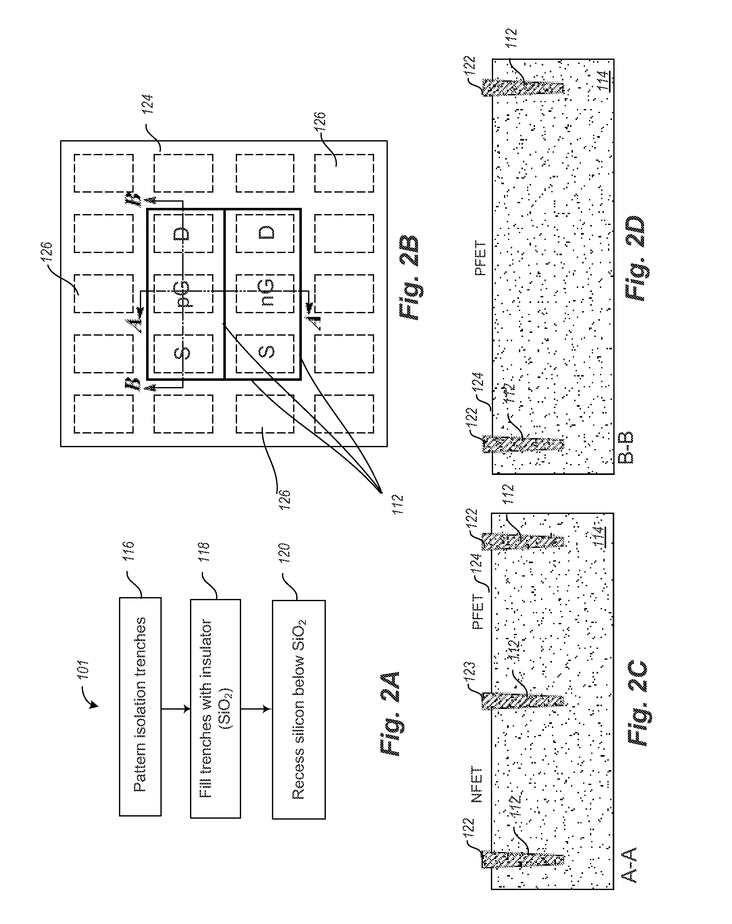
[0052]At 102, charge reservoirs in the source and drain regions are formed by doping areas of a silicon substrate between a pair of isolation trenches. A first method of doping uses conventional ion implantation. A second method of doping is performed in-situ during epitaxial growth.

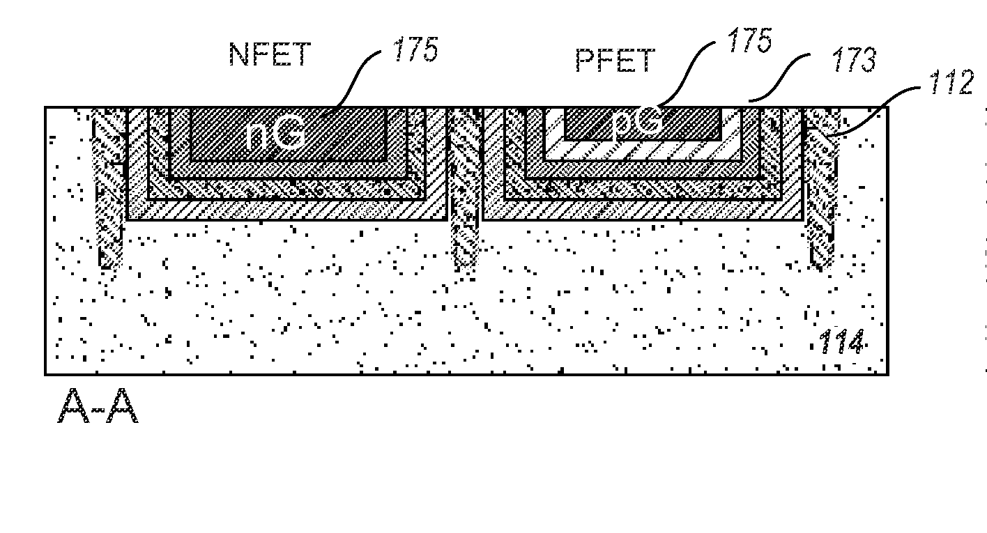
[0053]At 103, doped silicon is selectively removed from the gate region while remaining in the source and drain regions.

[0054]At 104, an epitaxial channel is formed between the source and drain regions.

[0055]At 106, a high-k gate is formed that includes a gate dielectric made of a material that has a high dielectric constant (e.g., halfnium oxide (HfO2), or Al2O3) and a metal gate electrode.

[0056]At 108, metal quantum dots are embedded in...

second embodiment

[0068]The ion implantation process shown and described in FIGS. 3A-3D is sometimes preferred for minimum dimensions (i.e., gate lengths) below 20 nm. At such small geometries, damage caused by ion implantation may result in severe degradation of the silicon crystalline structure in the source and drain regions. Sometimes the degradation is so great that it cannot be healed sufficiently by a later annealing process. In such cases, an alternative doping method can be substituted for ion implantation. One such alternative, source and drain doping during in-situ epitaxial growth, is presented as the process step 102, shown and described in detail in FIGS. 4A-4D.

[0069]FIG. 4A shows a sequence of process steps that can be used to form an epitaxial n-doped carrier reservoir 150 and epitaxial p-doped carrier reservoirs 155.

[0070]At 146, regions of the substrate 114 that are to be epitaxially doped in situ with negative ions (carrier reservoirs 150) are masked, preferably using a silicon nit...


PUM


Abstract

Metal quantum dots are incorporated into doped source and drain regions of a MOSFET array to assist in controlling transistor performance by altering the energy gap of the semiconductor crystal. In a first example, the quantum dots are incorporated into ion-doped source and drain regions. In a second example, the quantum dots are incorporated into epitaxially doped source and drain regions.

Description

RELATED APPLICATION[0001]This patent application claims benefit under 35 U.S.C. §119(e) of U.S. Provisional Patent Application No. 61 / 705,608, filed on Sep. 25, 2012, which is hereby incorporated by reference in its entirety.BACKGROUND[0002]1. Technical Field[0003]The present disclosure relates to the fabrication of nanometer-sized integrated circuit field effect transistor (FET) devices and, in particular, to devices that incorporate quantum dot films to control electrical characteristics of the devices.[0004]2. Description of the Related Art[0005]As technology nodes for integrated circuits scale below 10 nm, maintaining precise control of various electrical characteristics in bulk semiconductor devices becomes increasingly more challenging. Bulk semiconductor devices include, for example, metal-oxide-semiconductor field effect transistors (MOSFETs). A MOSFET is a three-terminal switching device that includes a source, a gate, and a drain. MOSFETs are interconnected by a network of...

Claims


Application Information

Patent Timeline
Patent Type & Authority Applications(United States)
IPC IPC(8): H01L29/775H01L29/66
CPCH01L29/66666H01L29/775H01L21/823814H01L21/823828H01L21/823842H01L27/092H01L29/165H01L29/401H01L29/413H01L29/41766H01L29/4236H01L29/456H01L29/4975H01L29/66431H01L29/7781H01L29/0653H01L29/127H01L29/41775H01L29/41783H01L29/42392H01L29/66621H01L29/66636H01L29/78618H01L29/78696
Inventor ZHANG, JOHN H.
Owner STMICROELECTRONICS INT NV
Why Eureka
Try Eureka