Multilayer ceramic electronic component

a technology of electronic components and ceramics, applied in the direction of fixed capacitor details, stacked capacitors, electrical apparatus construction details, etc., can solve the problems of increasing the number of processing units, increasing the number of cpus, and generating acoustic noise, etc., to prevent acoustic noise, ultra-high capacitance, and ultra-small siz

Inactive Publication Date: 2014-03-27
SAMSUNG ELECTRO MECHANICS CO LTD
View PDF6 Cites 8 Cited by
  • Summary
  • Abstract
  • Description
  • Claims
  • Application Information

AI Technical Summary

Benefits of technology

[0016]An aspect of the present invention provides a multilayer ceramic electronic component capable of preventing an acoustic sound generated at the time of being mounted on a printed circuit board and noise resulting therefrom, while implementing a product having an ultra-small size and ultra-high capacitance by decreasing margin portions and thicknesses of cover portions of dielectric layers as much as possible.

Problems solved by technology

Due to the recent trend in which display devices are relatively large, computer central processing units (CPUs) have been increased in speed, and the like, heat generation in electronic devices has become a serious issue.
Here, in the case in which thicknesses of margin portions and upper and lower cover portions of green sheets are excessively reduced, acoustic noise may be generated at the time of mounting the multilayer ceramic electronic component on a printed circuit board.

Method used


Image

  • Multilayer ceramic electronic component
  • Multilayer ceramic electronic component
  • Multilayer ceramic electronic component

Examples


Embodiment Construction

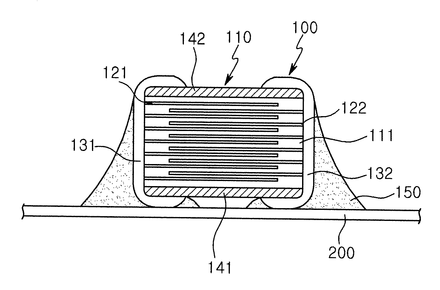
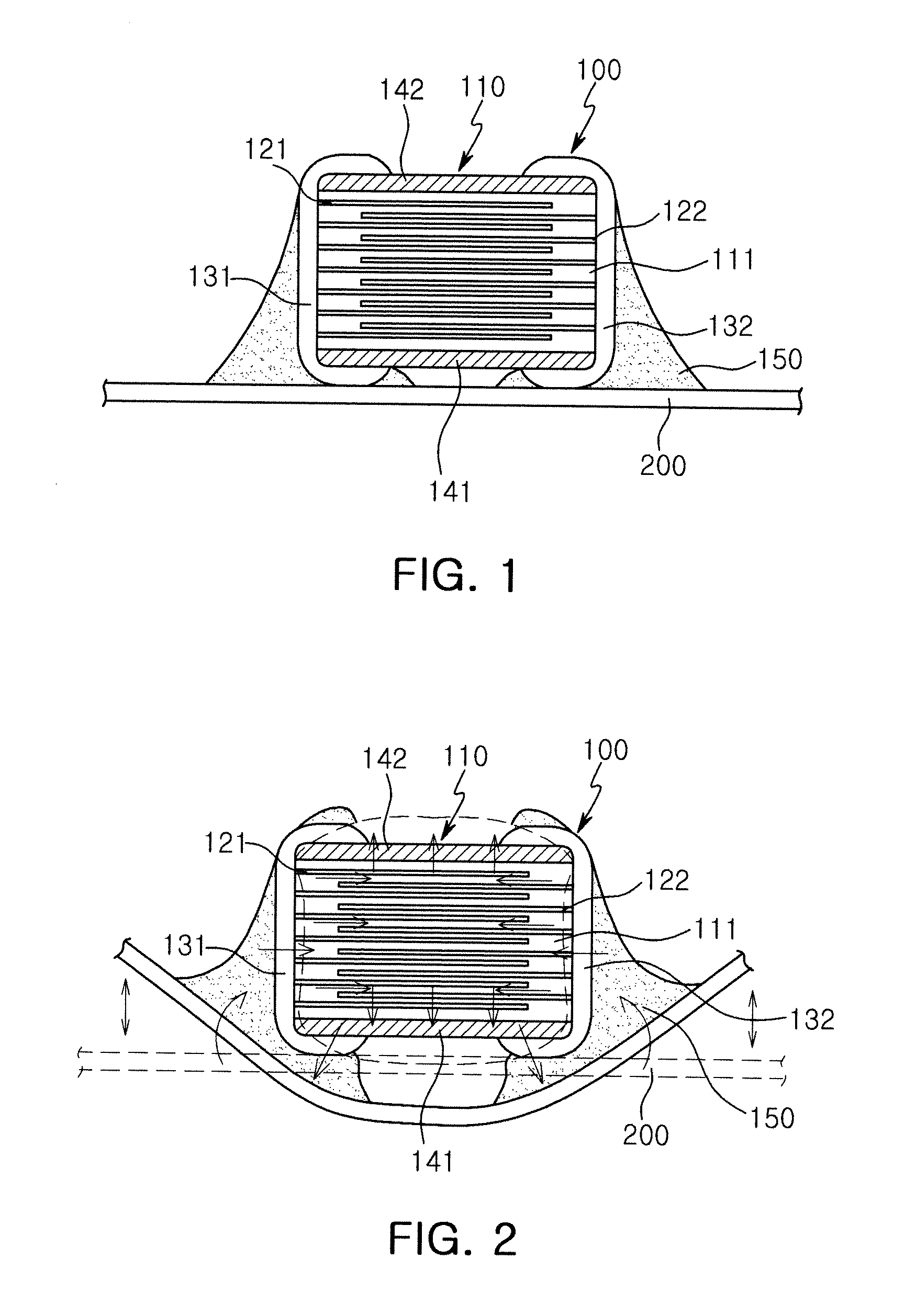
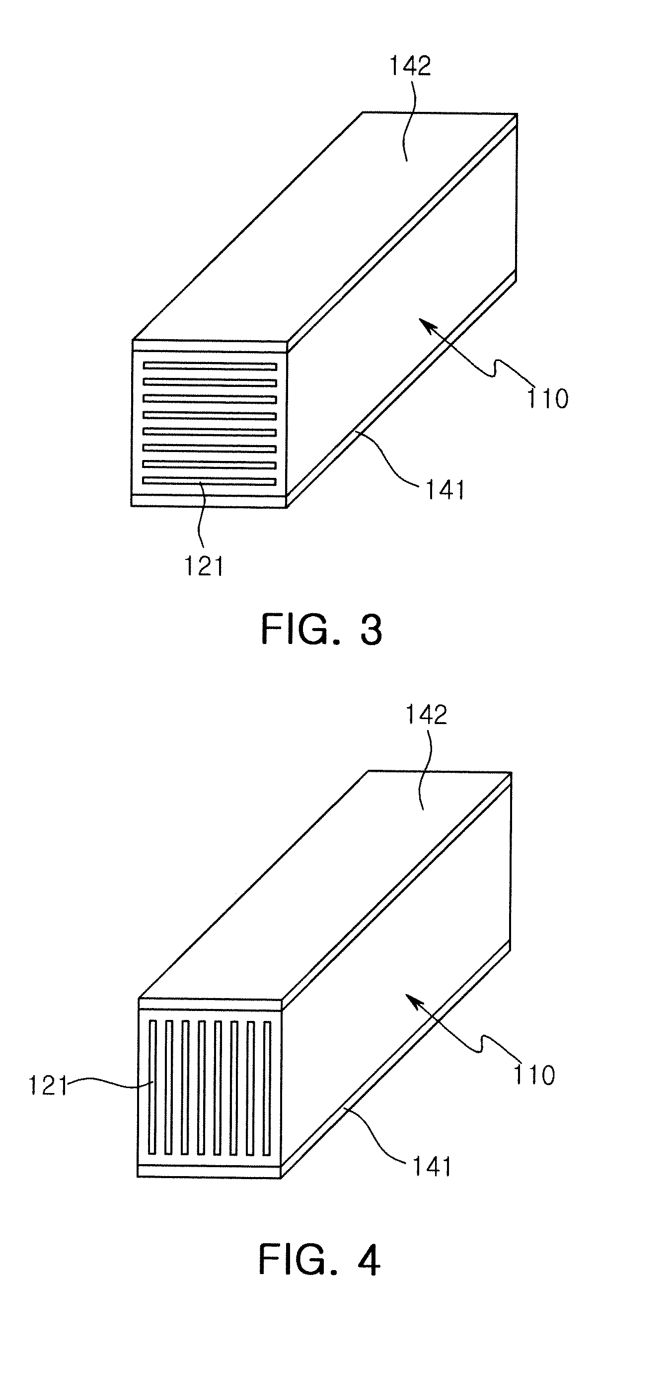
[0030]Hereinafter, embodiments of the present invention will be described in detail with reference to the accompanying drawings. The invention may, however, be embodied in many different forms and should not be construed as being limited to the embodiments set forth herein. Rather, these embodiments are provided so that this disclosure will be thorough and complete, and will fully convey the scope of the invention to those skilled in the art.

[0031]In the drawings, the shapes and dimensions of components may be exaggerated for clarity, and the same reference numerals will be used throughout to designate the same or like components.

[0032]The present invention relates to a multilayer ceramic electronic component, wherein the multilayer ceramic electronic component according to an embodiment of the present invention includes a multilayer ceramic capacitor, an inductor, a piezoelectric element, a varistor, a chip resistor, a thermistor, and the like. Hereinafter, the multilayer ceramic c...


PUM

PropertyMeasurementUnit
thicknessaaaaaaaaaa
capacitanceaaaaaaaaaa
sizeaaaaaaaaaa

Abstract

There is provided a multilayer ceramic electronic component including: a ceramic body in which a plurality of dielectric layers are stacked; a plurality of first and second internal electrodes formed on at least one surfaces of the dielectric layers and alternately exposed through both end surfaces of the ceramic body in a length direction of the ceramic body; a first acoustic noise absorption layer formed on one surface of the ceramic body in a stacking direction of the dielectric layers and having a thickness of 3 μm to 500 μm; first and second external electrodes formed on both end surfaces of the ceramic body and electrically connected to exposed portions of the first and second internal electrodes; and a printed circuit board having the first and second external electrodes mounted thereon while facing the first acoustic noise absorption layer.

Description

CROSS-REFERENCE TO RELATED APPLICATIONS[0001]This application claims the priority of Korean Patent Application No. 10-2012-0107928 filed on Sep. 27, 2012, in the Korean Intellectual Property Office, the disclosure of which is incorporated herein by reference.BACKGROUND OF THE INVENTION[0002]1. Field of the Invention[0003]The present invention relates to a multilayer ceramic electronic component.[0004]2. Description of the Related Art[0005]Provided as representative electronic components using a ceramic material are a capacitor, an inductor, a piezoelectric element, a varistor, a thermistor, and the like.[0006]Among ceramic electronic components, a multilayer ceramic capacitor (MLCC) has a small size, is able to secure high capacity, and has ease of mountability.[0007]A multilayer ceramic capacitor, a chip-type condenser, is installed in circuit boards of various electronic products including a display device such as a liquid crystal display (LCD), a plasma display panel (PDP), or th...

Claims


Application Information

Patent Timeline
Patent Type & Authority Applications(United States)
IPC IPC(8): H05K1/02
CPCH05K1/0216H01G2/065H05K3/3442H05K2201/10015H01G4/30H01G4/224H01G4/12
Inventor PARK, KYU SIKCHOI, JAE YEOLLEE, YOUNG SOOKPARK, MYUNG JUN
Owner SAMSUNG ELECTRO MECHANICS CO LTD
Why Eureka
Try Eureka