

Semiconductor device
- Summary
- Abstract
- Description
- Claims
- Application Information
AI Technical Summary
Benefits of technology
Problems solved by technology
Method used
Image

Examples
first embodiment
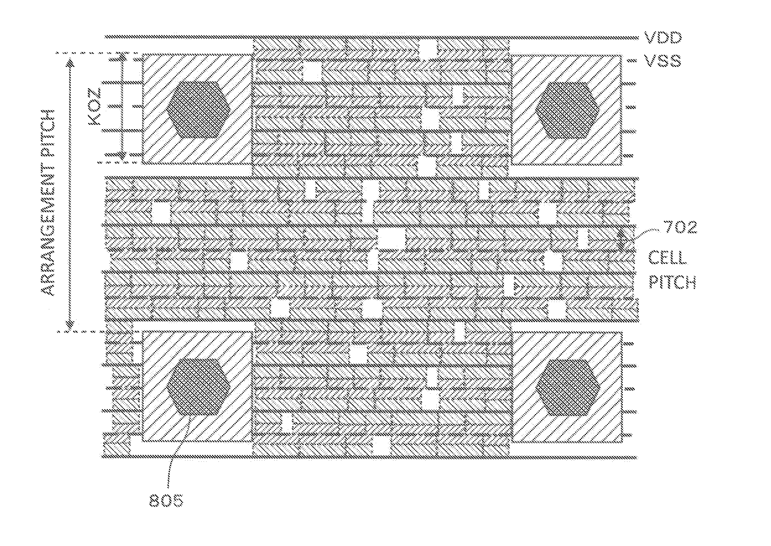
[0063]An explanation will be given of a first embodiment of the present invention as follows. The present embodiment is an example of arranging a TSV at a core circuit, and arranging a TSV having KOZ in a case where N=an even number in Equation (1) (in the present embodiment, N=6, 5h<a<6h). In a case of arranging a single piece of the TSV, as shown in FIG. 8, the TSV is arranged such that a center of the TSV is disposed on an extended line (which is not actually wired) of a power source (here, a second VSS line from top, or a second VSS line from bottom). An arrangement of a power source opposed to KOZ stays the same on upper and lower sides (here, VDD line). Generally, KOZ for NMOSFET is smaller than that of PMOSFET. Therefore, in a case where N can be made to be an even number, a VSS line is arranged to be opposed to the TSV. Plural TSVs are arranged, for example, as in FIG. 8. The arrangement pitch b of the TSV is made to be even number-fold of the cell pitch h, and made to be 12...
second embodiment
[0066]An explanation will be given of a second embodiment of the present invention as follows. The present example is an example of arranging a TSV to a core circuit, and arranging a TSV having KOZ in a case where N is an odd number in Equation (1). (In the present embodiment, N=3, 2h
[0067]In a case of arranging a single piece of TSV, the TSV is arranged such that a center of the TSV is disposed at a portion on an extended line of a power source similar to FIG. 8. An arrangement of the power source opposed to KOZ differs between upper and lower sides. Although N is preferably an even number inherently, in a case where a size of KOZ and a dead space cannot be reduced, such an arrangement is established. FIG. 11 is a view of arranging a TSV in a core circuit in a chip configuring a semiconductor device according to the present embodiment. Plural TSVs are arranged as shown in FIG. 11 (however, here, an example of arranging a center of the TSV on an extended line of a boundary li...
third embodiment
[0070]An explanation will be given of a third embodiment of the present invention as follows. The present example is other example of arranging a TSV in a core circuit as in the example of the second embodiment, and arranging a TSV having KOZ in which N is of a size of an odd number in Equation (1) (Here, N=3, 2h<a<3h). FIG. 13 is arrangement view of a TSV in a core circuit in a chip configuring a semiconductor device according to the present embodiment. As shown in FIG. 13, a minimum unit configuration is made by arranging at least 2 pieces of TSVs orthogonally to a direction of a power source line at an odd number-fold of a cell pitch (here, N=3) (here, a minimum unit is configured by 2 pieces of TSVs aligned in a cell pitch direction), and plural unit configurations thereof are arranged by even number-fold of the cell pitch (here, b≦8h). A coordinate of the unit configuration may be a coordinate of arranging one TSV configuring the unit configuration, or a gravitational center of...
PUM
 Abstract
Description
Claims
Application Information