Joining method using metal foam, method of manufacturing semiconductor device, and semiconductor device

a metal foam and metal foam technology, applied in the direction of metal-working apparatus, non-electric welding apparatus, solid-state devices, etc., can solve the problems of low speed of solid-liquid diffusion, insufficient heat resistance, and low temperature region, and achieve high thermal resistance, high reliability, and high thermal resistance

Inactive Publication Date: 2014-04-24
FUJI ELECTRIC CO LTD
View PDF11 Cites 37 Cited by
  • Summary
  • Abstract
  • Description
  • Claims
  • Application Information

AI Technical Summary

Benefits of technology

[0014]The thicknesses of the stacked films can be reduced in order to reduce the time required for solid-liquid diffusion, which makes the joined layers thin. In order to evenly adhere the surfaces to be joined to each other, the surfaces to be joined need to be extremely flat.
[0019]The present invention provides a joining method using a metal foam, which is capable of accomplishing highly thermally resistant and highly reliable joining, a method of manufacturing a semiconductor device by using the joining method, and a semiconductor device produced by the manufacturing method.
[0051]According to the present invention, a metal foam body is sandwiched between members to be joined. The members to be joined are brought into contact with each other and heated. In this heat treatment, a Sn film or other film of low-melting-point metal that covers the members to be joined is melted. Solid-liquid diffusion of Cu configuring the skeleton of the open cells of the metal foam body is caused in the molten Sn, to form an alloy layer, which is an intermetallic compound. At this stage, a Cu skeleton is left in the metal foam body. Then, the members to be joined are joined to each other by this alloy layer, achieving highly thermally resistant and highly reliable joining. With this joining method, a highly thermally resistant and highly reliable semiconductor device can be produced.
[0052]Furthermore, a semiconductor device of higher thermal resistant and reliability can be obtained by joining, directly or using brazing filler metal or Cu particles (nanoparticles), a surface on the opposite side to the surface facing a semiconductor chip, which is one of the members to be joined of the metal foam body, to the other one of the members to be joined, such as a lead frame and an insulating substrate with conductor patterns.

Problems solved by technology

However, the use of Pb is regulated in some regions on account of its harmful impact on the environment.
However, these solder members are used in low-temperature regions and medium-temperature regions and are not sufficiently heat resistant.
However, the speed of solid-liquid diffusion is normally low, and solid-liquid diffusion takes long time.
Therefore, the joining temperature needs to be raised, which makes the resultant intermetallic compound hard and fragile.

Method used


Image

  • Joining method using metal foam, method of manufacturing semiconductor device, and semiconductor device
  • Joining method using metal foam, method of manufacturing semiconductor device, and semiconductor device
  • Joining method using metal foam, method of manufacturing semiconductor device, and semiconductor device

Examples


example 1

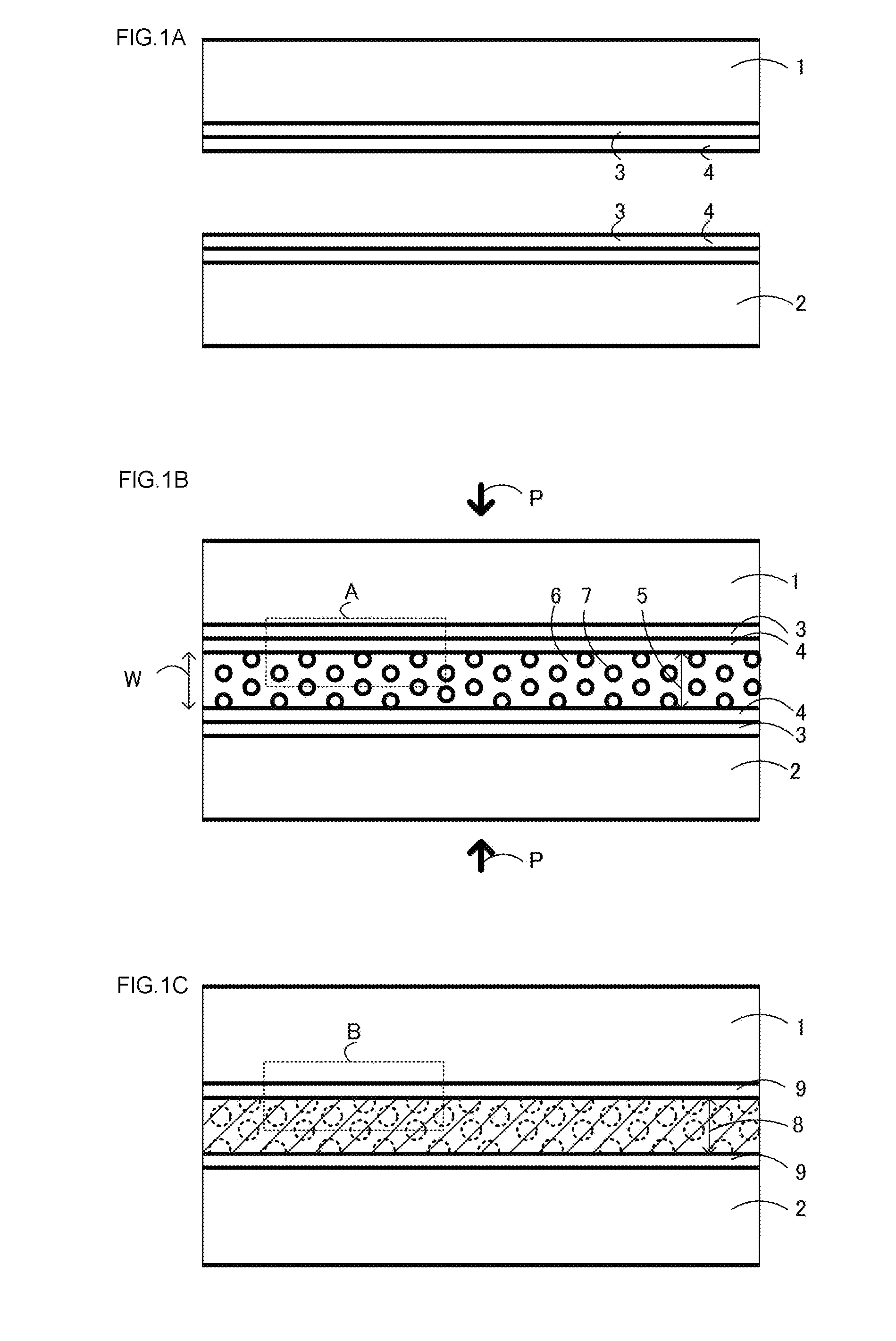
[0069]FIGS. 1A to 1C are cross-sectional diagrams sequentially showing main steps of a joining method using a metal foam according to a first example of the present invention.

[0070]In FIG. 1A, two Cu members to be joined 1, 2 are prepared. Ni film 3 is deposited onto each of the members to be joined 1, 2. Sn film 4 is then deposited thereon.

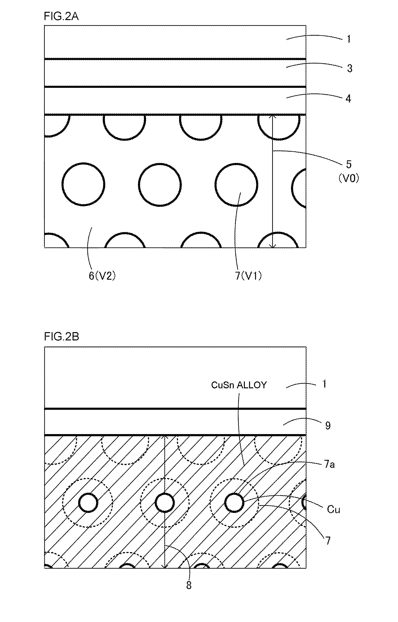
[0071]In FIG. 1B, Cu metal foam body 5 is placed between the two members to be joined 1, 2. The members to be joined 1, 2 are applied with pressure P and brought into contact with each other.

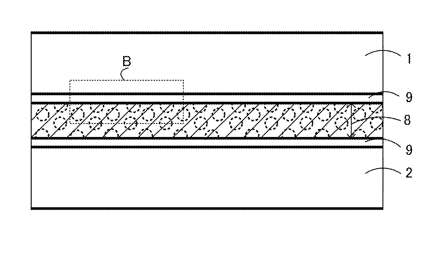
[0072]In FIG. 1C, the joined members are heated under pressure P in incubator 6 to melt the Sn of the members to be joined 1, 2 and solid-liquid diffuse the Cu of skeleton 7 of open cells 6 of metal foam body 5 in the Sn. This solid-liquid diffusion forms CuSn alloy layer 8 which is a metal compound. At this stage, Sn films 4 and Ni films 3 each form NiSn alloy layers 9 as intermetallic compounds. Due to slow reactions of the NiSn alloy layers 9, Ni films 3 m...

example 2

[0087]FIG. 3 is a cross-sectional diagram showing main steps of a joining method using a metal foam according to a second example of the present invention. The difference with FIG. 1 is that Sn film 4a is formed on skeleton 7 of Cu metal foam body 5. Sn film 4a may be formed by wet plating. When Sn film 4a is deposited on Cu skeleton 7 of open cells 6, Sn films 4 on the members to be joined 1, 2 and Sn film 4a on skeleton 7 melt and fuse together. When skeleton 7 is made of pure Cu, wettability of the Sn to the pure Cu becomes an issue; however, such an issue can be resolved. As a result, the Cu of metal foam body 5 can easily solid-liquid diffuse in the molten Sn of the members to be joined 1, 2, and consequently the Cu and the Sn react at a high speed, reducing the heat treatment time.

[0088]Of course, even when a Au film is formed in place of Sn film 4a by wet plating, wettability of Au can be improved, and the same effect can be accomplished thereby.

example 3

[0089]FIG. 4 is a cross-sectional diagram showing main steps of a joining method using a metal foam according to a third example of the present invention.

[0090]The difference between FIG. 1 and FIG. 3 is that Cu metal foam body 5 of this example is filled with Sn4b. The Sn4b is softened in open cells 6 by raising a temperature in advance near the melting (190° C.) point of the Sn4b and injected into open cells 6 of metal foam body 5.

[0091]At the stage of injecting the Sn4B into Cu metal foam body 5, the Cu and Sn4b in metal foam body 5 are simply in contact with each other without causing solid-liquid diffusion. Sn4b-filled Cu metal foam body 5 is held between the members to be joined 1, 2 covered by Sn films 4 and heated under the pressure P, to cause solid-liquid diffusion between the Sn4b and Cu, thereby joining the members to be joined 1, 2 together, with metal foam body 5 therebetween. In this case as well, the Sn of Sn films 4 on the members to be joined 1, 2 dissolves from th...


PUM

PropertyMeasurementUnit
pressureaaaaaaaaaa
pressureaaaaaaaaaa
melting-pointaaaaaaaaaa

Abstract

A joining method using a metal foam, a method of manufacturing a semiconductor device by using the joining method, and a semiconductor device produced by the manufacturing method are disclosed. A metal foam body is sandwiched between members to be joined, which are then brought into contact with each other and subjected to heat treatment. In this heat treatment, films of low-melting-point metal, such as Sn films covering the members to be joined, are melted. An alloy layer—an intermetallic compound—is formed by bringing about solid-liquid diffusion of Cu of a skeleton of open cells of the metal foam body in the molten Sn. At this stage, a Cu skeleton is left in the metal foam body. Highly thermally resistant and highly reliable joining can be realized by joining the members to be joined together by using this alloy layer.

Description

BACKGROUND OF THE INVENTION[0001]A. Field of the Invention[0002]The present invention relates to a joining method using metal foam, a method of manufacturing a semiconductor device such as a power semiconductor module in use of the joining method, and a semiconductor device produced by this manufacturing method.[0003]B. Description of the Related Art[0004]FIG. 9 is a cross-sectional diagram showing substantial parts of a conventional power semiconductor module. This power semiconductor module is mounted with a power semiconductor element such as an insulated gate bipolar transistor (IGBT).[0005]This power semiconductor module is configured by joining semiconductor chip 13 to insulating substrate 10, with solder member 23 therebetween, insulating substrate 10 being configured by a ceramic substrate and a conductor pattern (metal foil 12). The ceramic substrate contains aluminum oxide, aluminum nitride, silicon nitride and the like as base compounds. The conductor pattern is configure...

Claims


Application Information

Patent Timeline
Patent Type & Authority Applications(United States)
IPC IPC(8): H01L23/00B23K35/02
CPCH01L24/89H01L24/10B23K35/0233B23K35/02H01L2924/13055C22F1/16H01L2224/26125H01L24/29H01L24/32H01L24/83H01L2224/29076H01L2224/29082H01L2224/29111H01L2224/29147H01L2224/3201H01L2224/32507H01L2224/33181H01L2224/45124H01L2224/45144H01L2224/45147H01L2224/73215H01L2224/73265H01L2224/83007H01L2224/83065H01L2224/83075H01L2224/83097H01L2224/83101H01L2224/83193H01L2224/83203H01L2224/83447H01L2224/8381H01L2224/83815H01L2224/83825H01L2224/29155H01L2224/26155H01L2224/32225H01L2224/32245H01L2224/48227H01L2224/73104H01L2924/1305H01L2924/15747H01L2924/15787H01L2224/83192H01L2224/8384H01L2224/40225H01L24/40H01L2224/73221H01L2224/84801H01L24/37H01L2224/37124H01L2224/37147H01L2224/8385C04B37/02C04B37/026C04B2237/343C04B2237/365C04B2237/366C04B2237/368C04B2237/123C04B2237/124C04B2237/55C04B2237/60C04B2237/61C04B2237/86C04B37/006C04B2237/407H01L24/84H01L2224/2612H01L2924/00H01L2924/00014H01L2924/00012
Inventor TANIGUCHI, KATSUMI
Owner FUJI ELECTRIC CO LTD
Why Eureka
Try Eureka