Method and system for an adaptive negative-boost write assist circuit for memory architectures

a technology of write assist circuit and memory architecture, applied in the direction of information storage, static storage, digital storage, etc., can solve the problems of increasing process variation and device reliability, compromising device dimensions and threshold voltage targets established for sram devices, and imposing system level requirements. increasing constraints on sram designs

Inactive Publication Date: 2014-04-24
AVAGO TECH WIRELESS IP SINGAPORE PTE
View PDF1 Cites 35 Cited by
  • Summary
  • Abstract
  • Description
  • Claims
  • Application Information

AI Technical Summary

Benefits of technology

[0003]An embodiment of the invention may further comprise a system of producing capacitive coupling in a memory architecture, said system comprising a MUX select signal, an input data signal, a BOOST signal, a selected bitline, a write common node and a boost capacitor, wherein a write passgate turns on in response to the MUX select and

Problems solved by technology

In deep submicron technology nodes, increased process variation and device reliability issues place challenges in low power SRAM design.
With an ever increasing SRAM usage, and SRAM complexity, system level requirements are imposing increasing constraints on SRAM designs for improving key parame

Method used


Image

  • Method and system for an adaptive negative-boost write assist circuit for memory architectures
  • Method and system for an adaptive negative-boost write assist circuit for memory architectures
  • Method and system for an adaptive negative-boost write assist circuit for memory architectures

Examples


Embodiment Construction

[0008]The design of SRAM cells has traditionally involved a compromise between the read and write functions of the memory array to maintain cell stability, read performance and write performance. In particular, the transistors which make up the cross-coupled latch must be weak enough to be overdriven during a write operation, while also strong enough to maintain their data value when driving a bit-line during a read operation. The access transistors that connect the cross-coupled inverters to the true and complement bit-lines affect both the stability and performance of the cell. It is understood that while the description of the invention may refer to SRAM type memories, the invention is not limited to SRAM. The techniques, methods and systems disclosed herein are equally applicable to other memory types, such as CAM and other memory architectures.

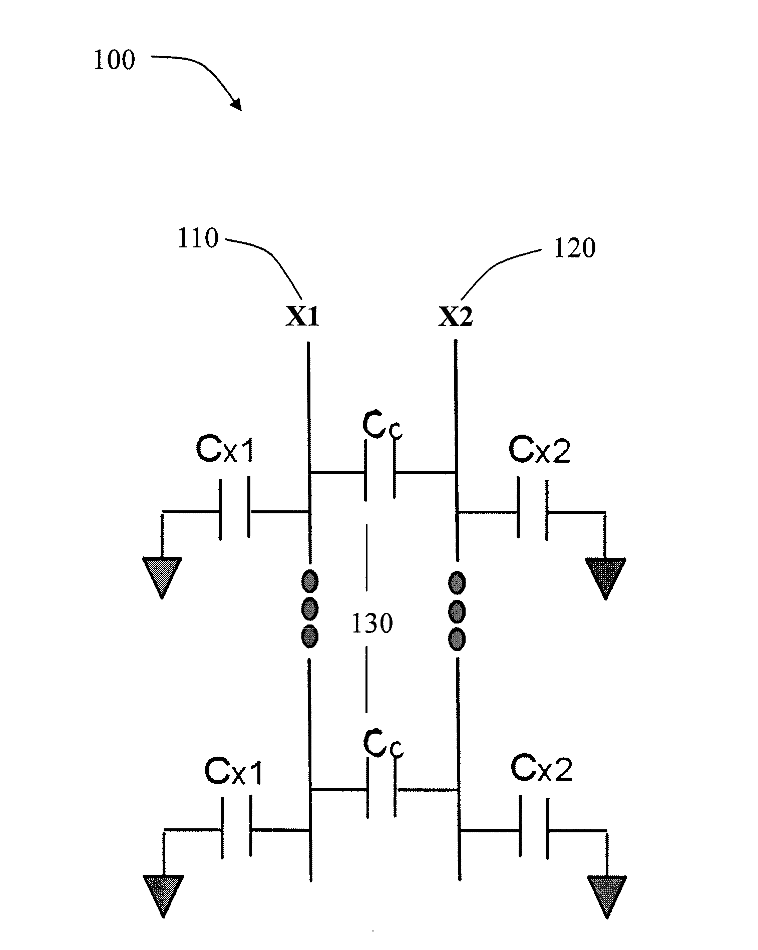
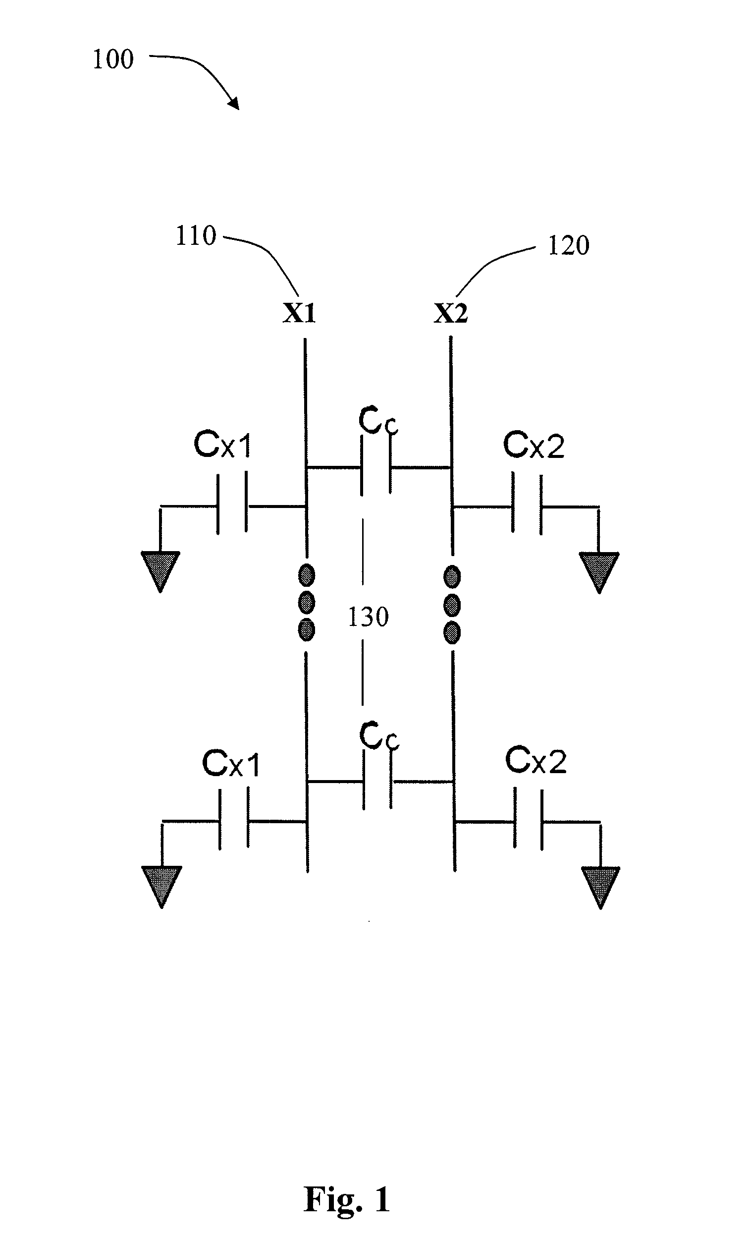
[0009]FIG. 1 is a capacitive coupling boost capacitor. There are two coupling lines in the layout 100, X1 110 and X2 120. Capacitor Cc 1...


PUM


Abstract

Disclosed is an adaptive negative bit-line boost write assist technique in which coupling capacitance scales with the number of rows and thereby maintains a constant negative bit-line level. The change in the coupling capacitance in neighboring signals as the height increases is utilized. The change is utilized for negative bit-line voltage generation.

Description

BACKGROUND OF THE INVENTION[0001]In deep submicron technology nodes, increased process variation and device reliability issues place challenges in low power SRAM design. SRAMs occupy up to or more than 70% of the SoC area and therefore, SRAM area, power, performance and leakage are significant deciding factors in overall budgeting of SoC. With an ever increasing SRAM usage, and SRAM complexity, system level requirements are imposing increasing constraints on SRAM designs for improving key parameters like area, speed, leakage, dynamic power, etc. A unique feature of SRAMs, such as a 6 transistor SRAM, is an inherent trade-off between stability when holding data during a read or non-column selected write access and the ability of the cell to be written. This means that device dimensions and threshold voltage targets established for SRAM devices are compromise by design. The ability to read and write is characterized in terms of margins to assess the functional implications. It is diff...

Claims


Application Information

Patent Timeline
IPC IPC(8): G11C11/00
CPCG11C11/419
Inventor TRIVEDI, MANISHGOEL, ANKURRAO, SETTI SHANMUKHESWARA
Owner AVAGO TECH WIRELESS IP SINGAPORE PTE
Why Eureka
Try Eureka