Multi-Master Cache Coherent Speculation Aware Memory Controller with Advanced Arbitration, Virtualization and EDC

a memory controller and multi-master technology, applied in computing, instruments, climate sustainability, etc., can solve problems such as stalling out other cores real accesses, affecting the real access of other cores, and breaking coherency, etc., to achieve low latency/bandwidth penalty, high bandwidth access, and low latency access

Active Publication Date: 2014-04-24
TEXAS INSTR INC
View PDF2 Cites 19 Cited by
  • Summary
  • Abstract
  • Description
  • Claims
  • Application Information

AI Technical Summary

Benefits of technology

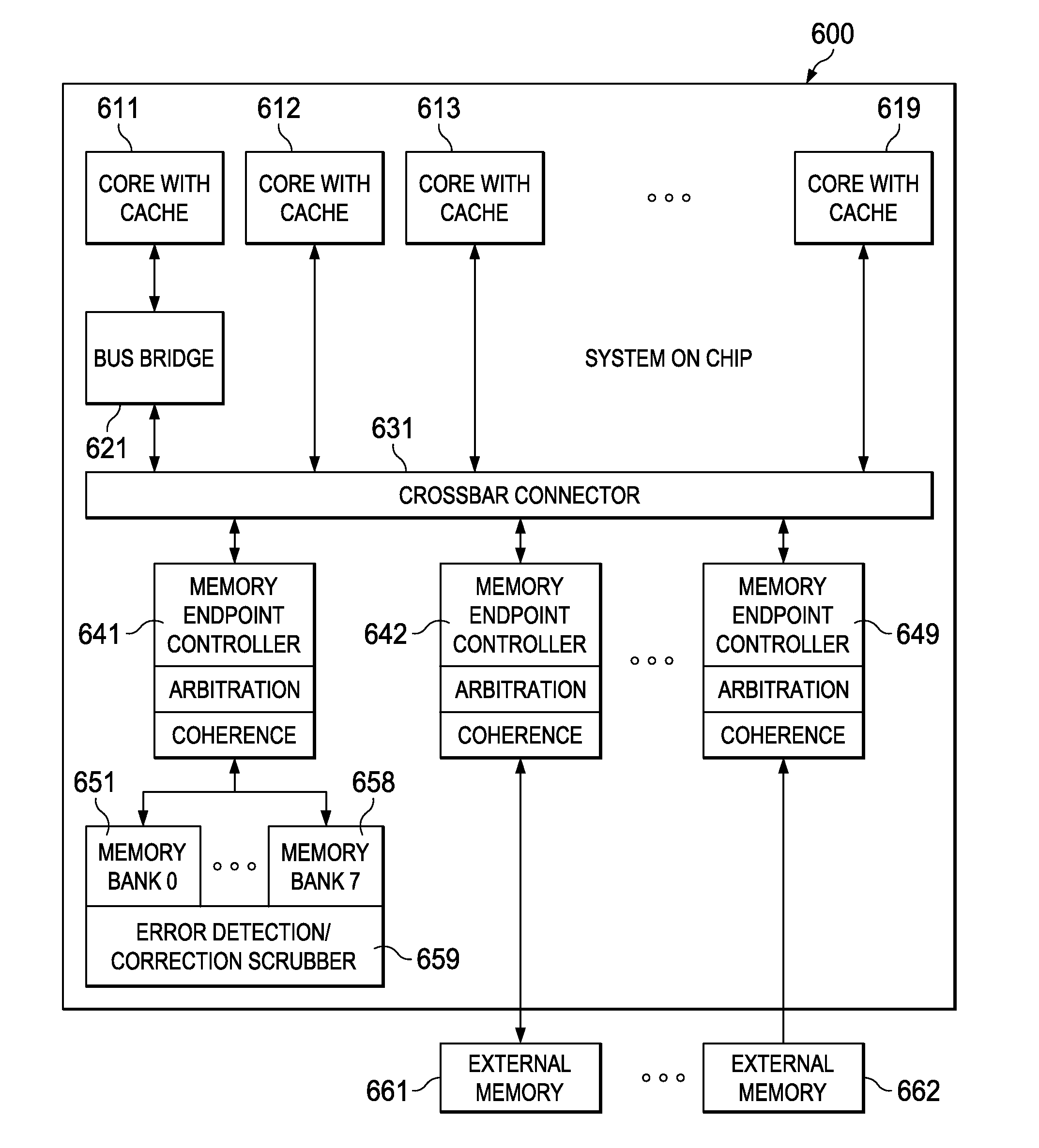
[0009]This invention integrates all of these features into a single unified interconnect between processors and memory endpoints. Most interconnect solutions provide just a connection infrastructure between masters and slaves. Integrating some of the controller / interconnect features into a single package minimizes the latency / bandwidth penalty of providing these features discreetly.
[0010]This invention advantageously provides a full crossbar interconnect between masters and memory endpoints provides extremely high-bandwidth, low-latency access from all masters to all slaves. The full crossbar ensures that masters accessing different endpoints do not interfere with each other. This invention has LS banked on-chip SRAM controllers provide very high bandwidth access to very large on-chip memories. The LS banking allows the software to take full advantage of the hardware without specific knowledge of the memory bank layout. This invention includes an integrated off-chip memory controller which provides a low-latency port to a high-capacity external memory. This invention includes distributed hardware coherence for all of the memory endpoints greatly reduces the software complexity of a multi-core system. The coherence hardware can also be disabled possibly resulting in a higher performing system. This invention includes a complex arbitration scheme allows users to prioritize system traffic as necessary and at the same time ensure no single master is completely starved. Virtualization reduces software complexity and ease of migration to future devices. The memory protection hardware provides both advisory and strict security checks enabling secure applications. Error detection and correction hardware minimizes FITs (Failures-In-Time) resulting from on-chip memory corruption. Automated scrubbing hardware also works in the background to eliminate corrupted memory locations without software intervention.

Problems solved by technology

This situation could break coherency, if DMA data were committed incorrectly.
Several issues arise.
At deep sub-micron geometries memory cells are very susceptible to soft errors which could lead to incorrect calculations or crashes.
If one core is highly speculative and floods the system with these accesses it could stall out other cores real accesses.

Method used


Image

  • Multi-Master Cache Coherent Speculation Aware Memory Controller with Advanced Arbitration, Virtualization and EDC
  • Multi-Master Cache Coherent Speculation Aware Memory Controller with Advanced Arbitration, Virtualization and EDC
  • Multi-Master Cache Coherent Speculation Aware Memory Controller with Advanced Arbitration, Virtualization and EDC

Examples


Embodiment Construction

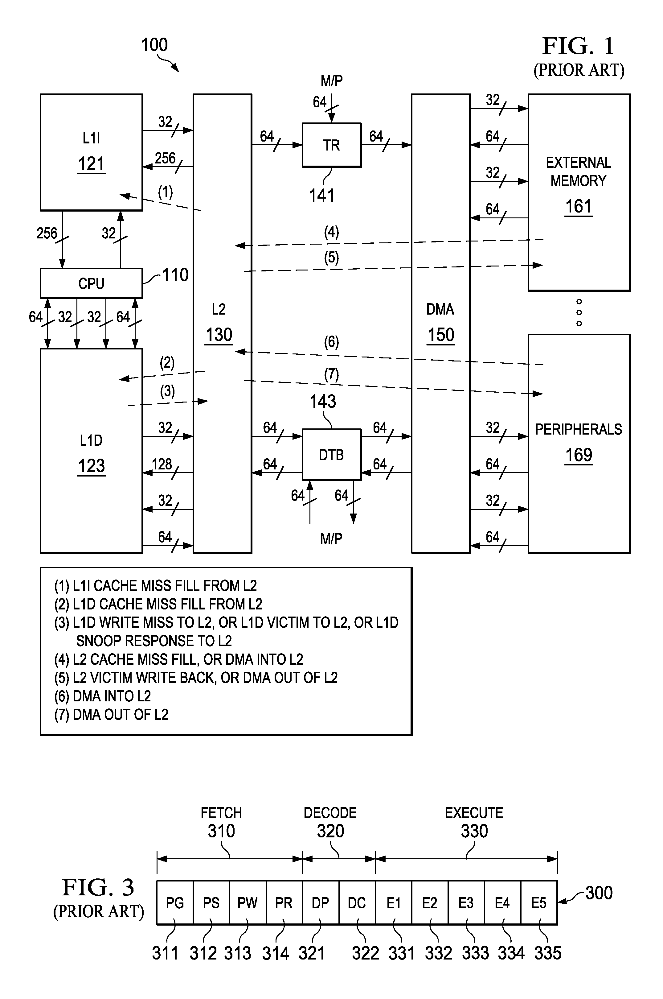
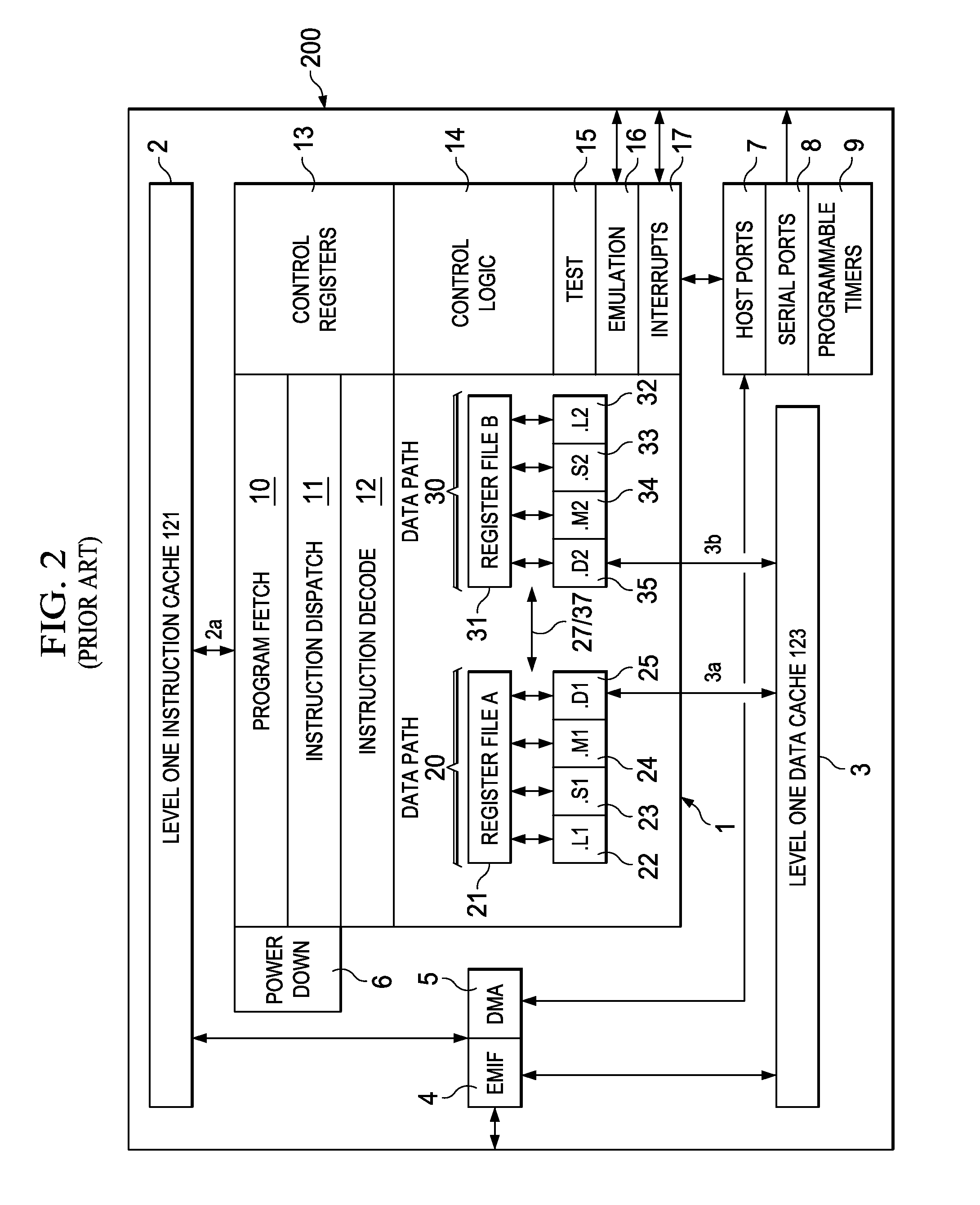
[0025]FIG. 1 illustrates the organization of a typical digital signal processor system 100 to which this invention is applicable (prior art). Digital signal processor system 100 includes central processing unit core 110. Central processing unit core 110 includes the data processing portion of digital signal processor system 100. Central processing unit core 110 could be constructed as known in the art and would typically include a register file, an integer arithmetic logic unit, an integer multiplier and program flow control units. An example of an appropriate central processing unit core is described below in conjunction with FIGS. 2 to 4.

[0026]Digital signal processor system 100 includes a number of cache memories. FIG. 1 illustrates a pair of first level caches. Level one instruction cache (L1I) 121 stores instructions used by central processing unit core 110. Central processing unit core 110 first attempts to access any instruction from level one instruction cache 121. Level one...


PUM


Abstract

This invention is an integrated memory controller/interconnect that provides very high bandwidth access to both on-chip memory and externally connected off-chip memory. This invention includes an arbitration for all memory endpoints including priority, fairness, and starvation bounds; virtualization; and error detection and correction hardware to protect the on-chip SRAM banks including automated scrubbing.

Description

CLAIM OF PRIORITY[0001]This application claims priority under 35 U.S.C. 119(e)(1) to U.S. Provisional Application No. 61 / 717,872 filed Oct. 24, 2012.TECHNICAL FIELD OF THE INVENTION[0002]The technical field of this invention is cache for digital data processors.BACKGROUND OF THE INVENTION[0003]This invention is applicable to data processing systems with multi-level memory where the second level (L2) memory used for both unified (code and instructions) level two cache and flat (L2 SRAM) memory used to hold critical data and instructions. The second level memory (L2) is used for multiple purposes including unified instruction and data level two cache, directly addressable SRAM memory used to hold critical data and code accessible by both external and internal direct memory access (DMA) units.[0004]When the level one data cache controller is granted access to the level one data cache, this access could force an existing line to be evicted. The CPU can also force the level one data cach...

Claims


Application Information

Patent Timeline
Patent Type & Authority Applications(United States)
IPC IPC(8): G06F13/16
CPCG06F13/1663G06F13/1626G06F12/0828G06F12/0831H04L63/0263G06F13/42G06F13/287G06F13/4022Y02D10/00G06F12/0815G06F21/79G06F21/78G06F12/1458G06F12/1491G06F13/1605G06F13/30G06F12/0835G06F12/1081G06F2212/621G06F12/0842G06F2212/1032G06F2212/283G06F2212/62
Inventor CHIRCA, KAIPIERSON, MATTHEW D.ANDERSON, TIMOTHY D.
Owner TEXAS INSTR INC
Why Eureka
Try Eureka