Current Redistribution in a Printed Circuit Board

a technology of printed circuit board and current, applied in the direction of printed circuit non-printed electric components association, electrical apparatus contruction details, cad circuit design, etc., can solve the problems of high resistance drop, open circuit, or brownout, and delamination of the pcb

Active Publication Date: 2014-05-01
CISCO TECH INC
View PDF22 Cites 21 Cited by
  • Summary
  • Abstract
  • Description
  • Claims
  • Application Information

AI Technical Summary

Problems solved by technology

The increasing high current can cause burnouts, open circuits, or brownouts because adequate area is not available on the PCB for power supply.
Further, such current crowding leads to high resistance (IR) drop.
The increased IR drops cause additional thermal heat, which may cause de-lamination of the PCB.
In addition, some high density PCBs have limited spa

Method used


Image

  • Current Redistribution in a Printed Circuit Board
  • Current Redistribution in a Printed Circuit Board
  • Current Redistribution in a Printed Circuit Board

Examples


example embodiments

[0021]A challenge in high end routing platforms is printed circuit board (PCB) density. Each generation of electronics demands significant increases in current, yet PCB space generally stays the same. The resulting increase in current density pushes the limits of through hole vertical interconnect accesses (vias) near load devices, such as voltage regulator modules. Due to positioning, different load devices may undesirably receive different amounts of current. The relative current distribution depends on the resistance from source to load. Selectively increasing the resistance in a path redistributes the current. The following embodiments include techniques to selectively redistribute current in a power plane of the PCB.

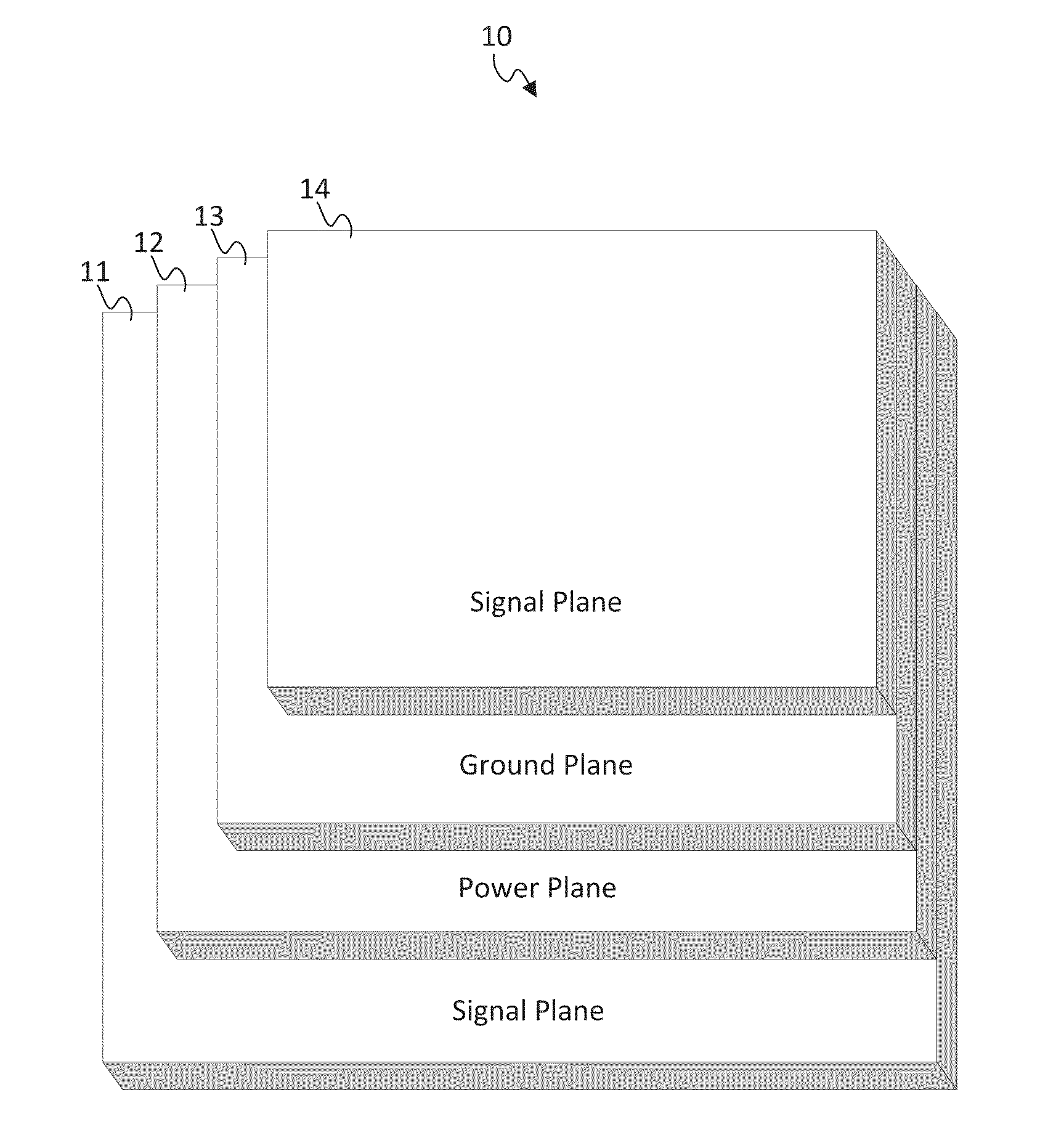
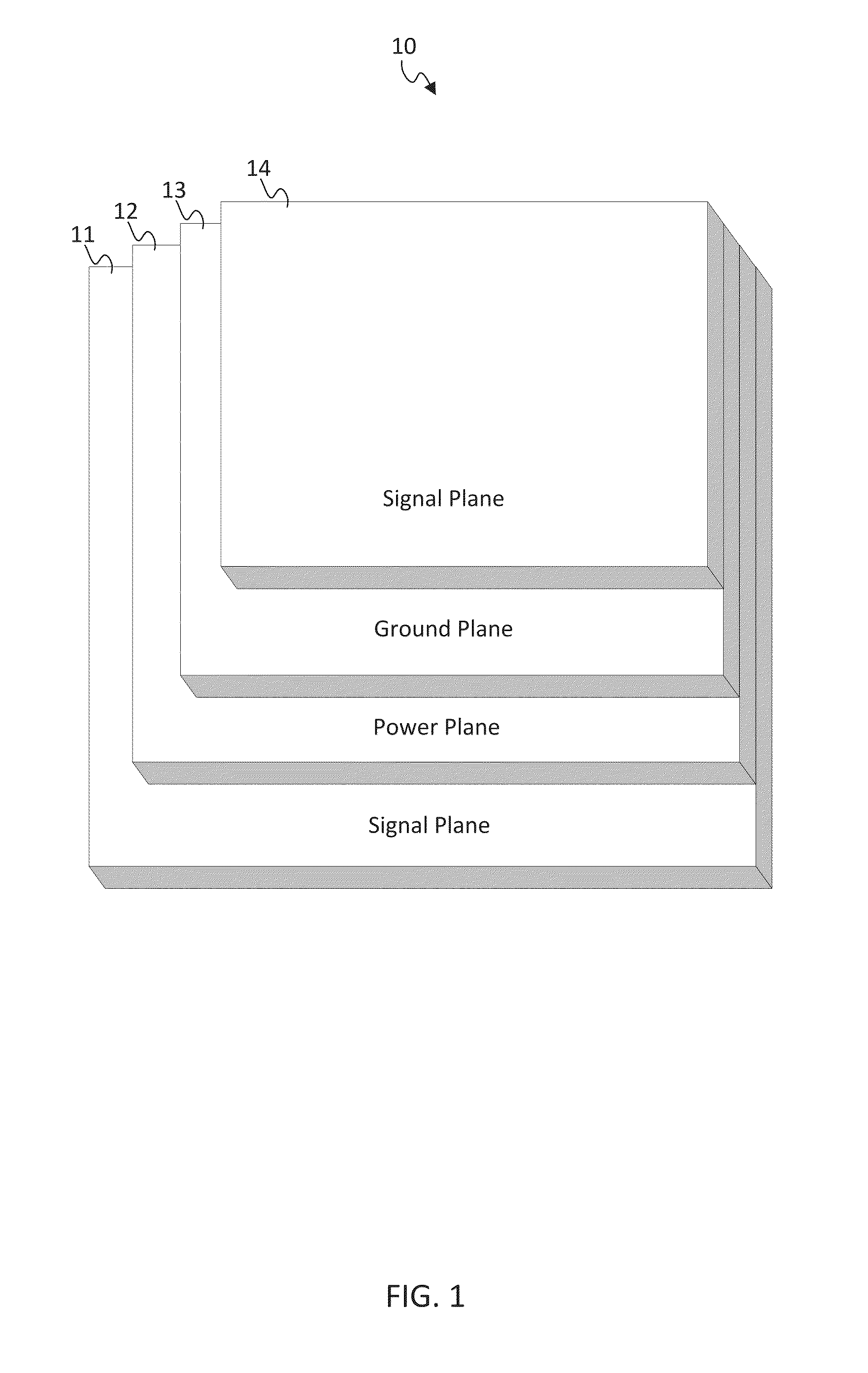
[0022]FIG. 1 illustrates a multilayered printed circuit board 10. The multilayered printed circuit board 10 may have any number and / or types of layers or planes. The multilayered printed circuit board 10 shown in FIG. 1 includes a first signal plane 11, a power plan...


PUM


Abstract

In one implementation, a multilayered printed circuit board is configured to redirect current distribution. The current may be distributed by steering, blocking, or otherwise manipulating current flows. The multilayered printed circuit board includes at least one power plane layer. The power plane layer does not distribute current evenly. Instead, the power plane layer includes multiple patterns with different resistances. The patterns may include a hatching pattern, a grid pattern, a directional pattern, a slot, a void, or a continuous pattern. The pattern is a predetermined spatial variation such that current flows in a first area differently than current flows in a second area.

Description

TECHNICAL FIELD[0001]This disclosure relates in general to the field of printed circuit boards, more particularly, to printed circuit boards with high current applications.BACKGROUND[0002]A printed circuit board (PCB) is used in nearly every consumer and industrial electronic device. The PCB structurally supports multiple electronic components. Traces on the PCB supply signals to the electronic components. A PCB may have a one-sided single layer, a double-sided single layer, or multiple layers. PCBs with multiple layers have one or more layers of “printed” circuits separated by one or more layers of insulation. The electronic components on the surface connect through plated holes drilled down to a specific layer of printed circuit.[0003]The increasing high current can cause burnouts, open circuits, or brownouts because adequate area is not available on the PCB for power supply. Further, such current crowding leads to high resistance (IR) drop. The increased IR drops affects the powe...

Claims


Application Information

Patent Timeline
IPC IPC(8): H05K1/18H05K1/11H05K1/02
CPCH05K1/0265H05K2201/09681H05K2201/0969H05K2201/093H05K1/0224H05K1/0298G06F30/30G06F30/39G06F30/367G06F2115/12H05K3/225
Inventor SABAVAT, GOUTHAMMOHAMED, JAVIDRAMANATHAN, SUBRAMANIANSCEARCE, STEPHEN A.
Owner CISCO TECH INC
Why Eureka
Try Eureka