Programmable logic device with integrated network-on-chip

a logic device and network-on-chip technology, applied in the field of programmable logic devices with integrated network-on-chip, can solve the problems of inefficient devices, inefficient wire use, and inefficiency of devices

Active Publication Date: 2014-05-08
ALTERA CORP
View PDF3 Cites 67 Cited by
  • Summary
  • Abstract
  • Description
  • Claims
  • Application Information

AI Technical Summary

Benefits of technology

[0006]This disclosure relates to integrated circuit devices, and, particularly, to such devices having a progr

Problems solved by technology

Such existing routing methods may render the device inefficient, e.g., when the routing is not used every cycle.
A first form of inefficiency occurs because of inefficient wire use.
In a first example, when an A-to-B connection is rarely used (for example, if the signal value generated by the source logic area at A rarely changes or the destination logic area at B is rarely programmed to be affected by the result), then the conductors used to implement the A-to-B connection may unnecessarily take up metal, power, and/or logic resources.
In a second example, when a multiplexed bus having N inputs is implemented in a point-to-point fashion, metal resources may be wasted on routing data from each of the N possible input wires because the multiplexed bus, by definition, outputs only one of the N input wires and ignores the other N−1 input wires.
Power resources may also be wasted in these examples when spent in conn

Method used


Image

  • Programmable logic device with integrated network-on-chip
  • Programmable logic device with integrated network-on-chip
  • Programmable logic device with integrated network-on-chip

Examples


Embodiment Construction

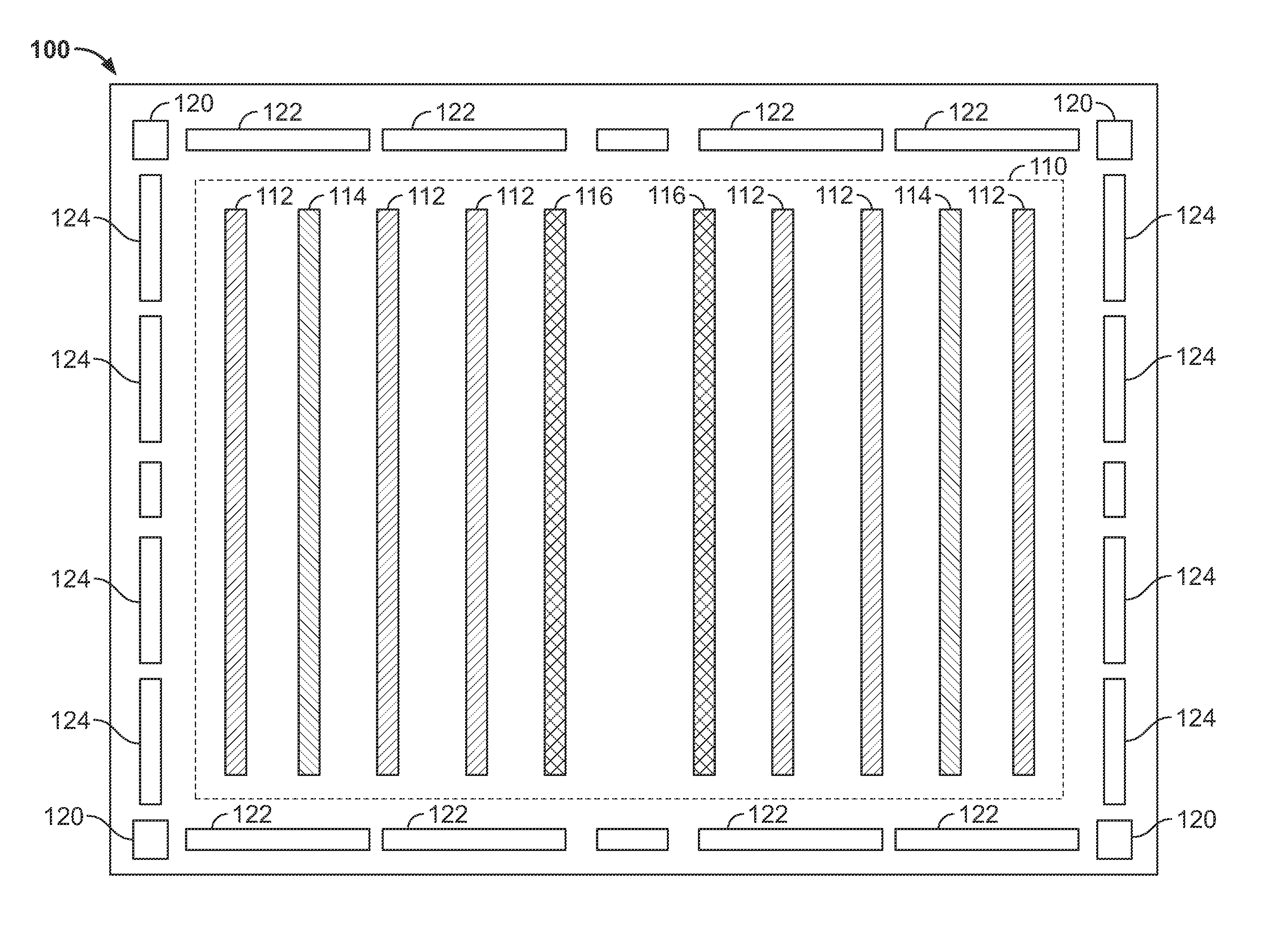
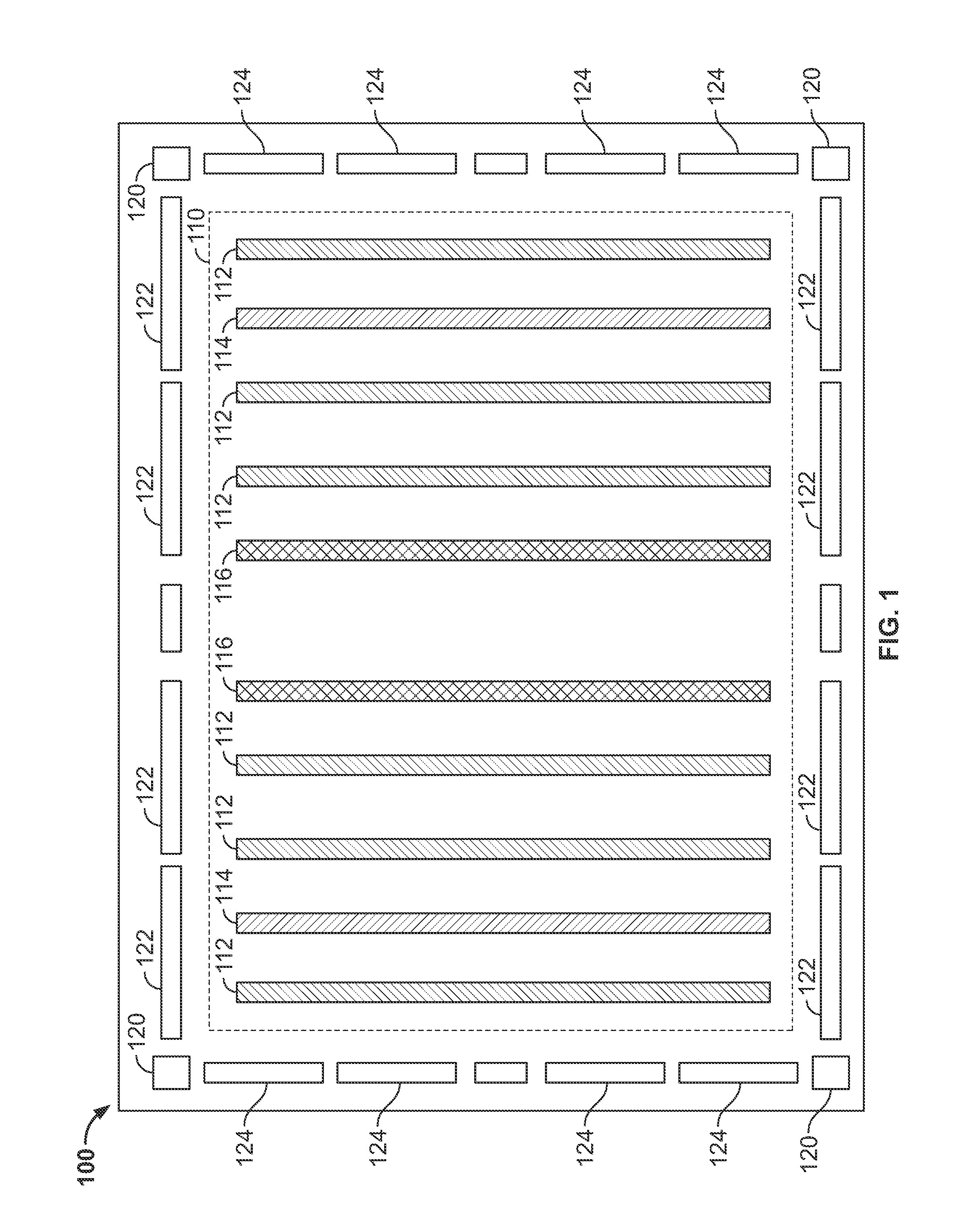
[0029]FIG. 1 depicts an illustrative floorplan 100 of an FPGA in accordance with an implementation. The floorplan 100 depicts various illustrative blocks of an FPGA. The floorplan 100 includes core logic fabric 110, which may have configurable logic blocks, look-up tables (LUTs), and / or D flip-flops (DFFs) (not explicitly shown in FIG. 1). The floorplan 100 includes memory blocks 112 and memory block 116. The memory blocks 112 may each be of a different bit size than the memory blocks 116. For example, in one arrangement, each of the memory blocks 112 is a 512-bit memory block, while each of the memory blocks 116 is a 4,096-bit memory block. The floorplan 100 includes variable-precision digital signal processing (DSP) blocks 114. In some arrangements, each DSP block of the DSP blocks 114 includes a number of multipliers, adders, subtractors, accumulators, and / or pipeline registers.

[0030]The floorplan 100 includes phase lock loops (PLLs) 120 and general purpose input-output (I / O) int...


PUM


Abstract

Systems and methods for providing a Network-On-Chip (NoC) structure on an integrated circuit for high-speed data passing. In some aspects, the NoC structure includes multiple NoC stations with a hard-IP interface having a bidirectional connection to local components of the integrated circuit. In some aspects, the NoC stations have a soft-IP interface that supports the hard-IP interface of the NoC station.

Description

CROSS-REFERENCE TO RELATED APPLICATIONS[0001]This application claims the benefit of, and priority to, U.S. Provisional Application No. 61 / 721,844, filed Nov. 2, 2012, the disclosure of which is incorporated herein by reference in its entirety.BACKGROUND OF THE DISCLOSURE[0002]Existing integrated circuits such as programmable logic devices (PLDs) typically utilize “point-to-point” routing, meaning that a path between a source signal generator and one or more destinations is generally fixed at compile time. For example, a typical implementation of an A-to-B connection in a PLD involves connecting logic areas through an interconnect stack of pre-defined horizontal wires. These horizontal wires have a fixed length, are arranged into bundles, and are typically reserved for that A-to-B connection for the entire operation of the PLD's configuration bitstream. Even where a user is able to subsequently change some features of the point-to-point routing, e.g., through partial recompilation, s...

Claims


Application Information

Patent Timeline
IPC IPC(8): H04L12/931H04L47/80
CPCH04L49/35H04L49/109H04L41/0894H04L41/12G06F15/7825H04L41/0893H04L47/805
Inventor HUTTON, MICHAEL DAVIDSCHMIT, HERMAN HENRYHOW, DANA
Owner ALTERA CORP
Why Eureka
Try Eureka