Method for manufacturing light emitting device and light emitting device

a technology of light emitting devices and manufacturing methods, applied in semiconductor devices, semiconductor/solid-state device details, electrical devices, etc., can solve problems such as degradation of light quality, and achieve the effect of improving light-extraction efficiency and increasing the thickness of the reflective layer

Active Publication Date: 2014-05-15
NICHIA CORP
View PDF6 Cites 97 Cited by
  • Summary
  • Abstract
  • Description
  • Claims
  • Application Information

AI Technical Summary

Benefits of technology

[0009]Accordingly, it is an object of the present invention to provide a method for manufacturing a light emitting device, and a light emitting device manufactured by the method that can improve the light-extraction efficiency by suppressing the sink of the reflective resin and increasing the thickness of the reflective layer on the side surface of the phosphor layer.
[0014]Accordingly, the invention can provide a light emitting device with improved light-extraction efficiency by increasing the thickness of the reflective layer on the side surface of the phosphor layer by suppressing the sink of the reflective resin.

Problems solved by technology

This might make the light emitted from a light emitting surface non-uniform, or render an end of the light emitting surface vague, thus leading to degradation of light quality.

Method used


Image

  • Method for manufacturing light emitting device and light emitting device
  • Method for manufacturing light emitting device and light emitting device
  • Method for manufacturing light emitting device and light emitting device

Examples


first embodiment

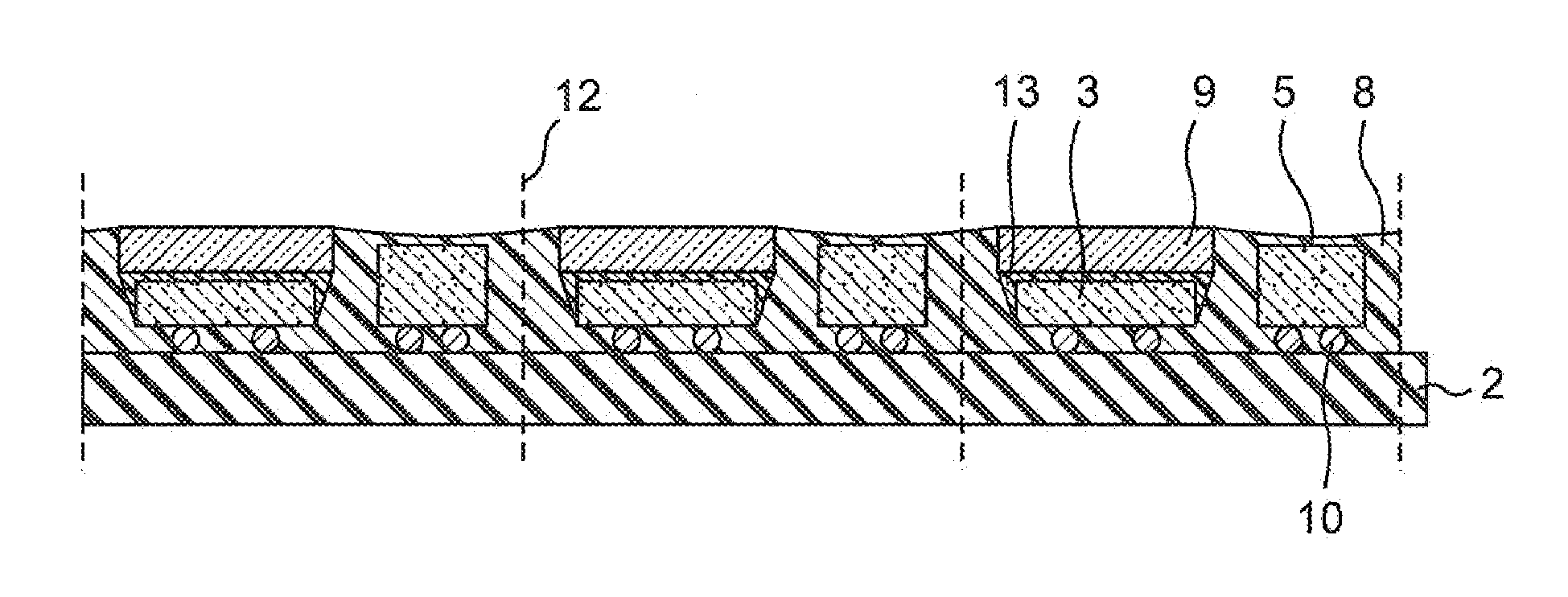
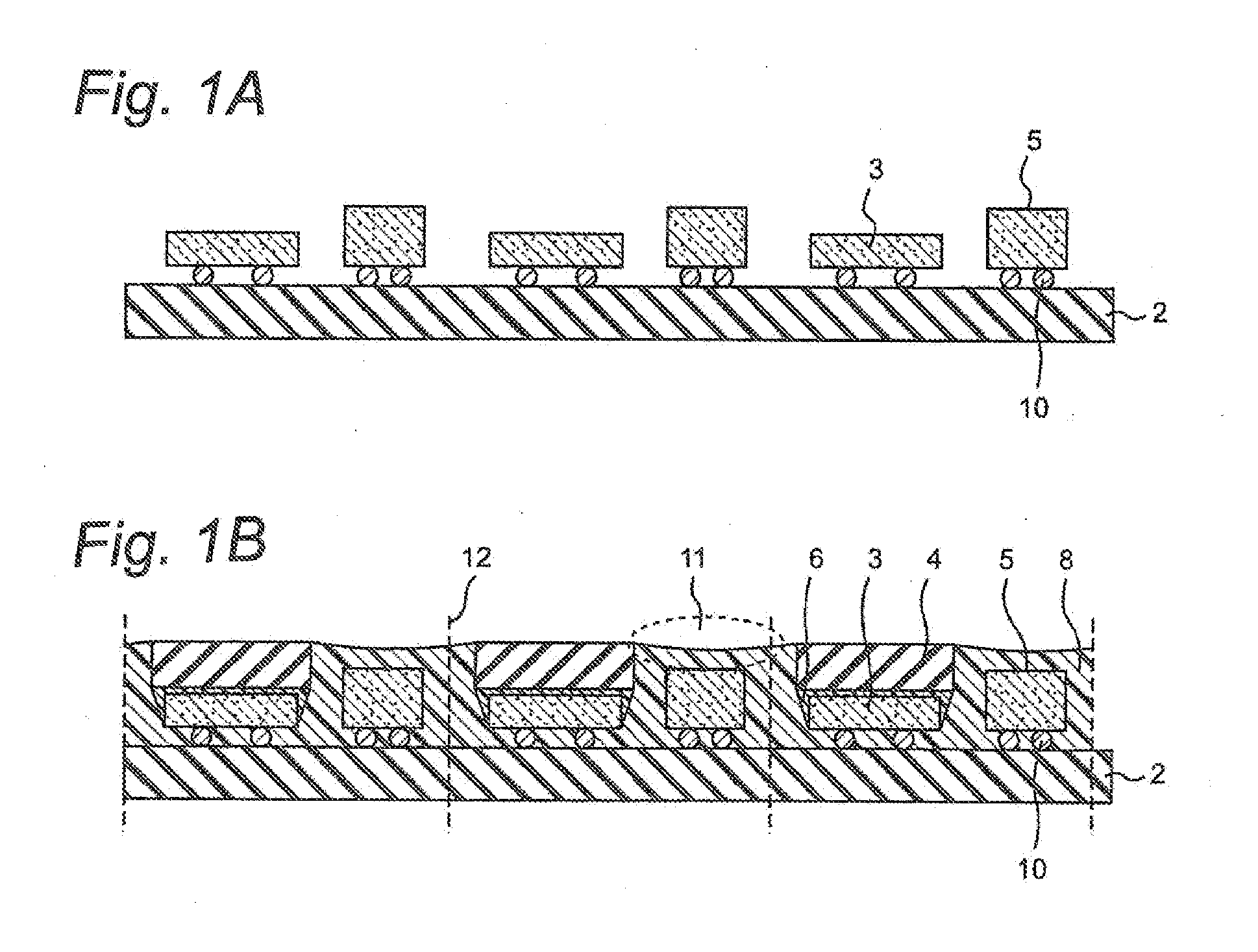
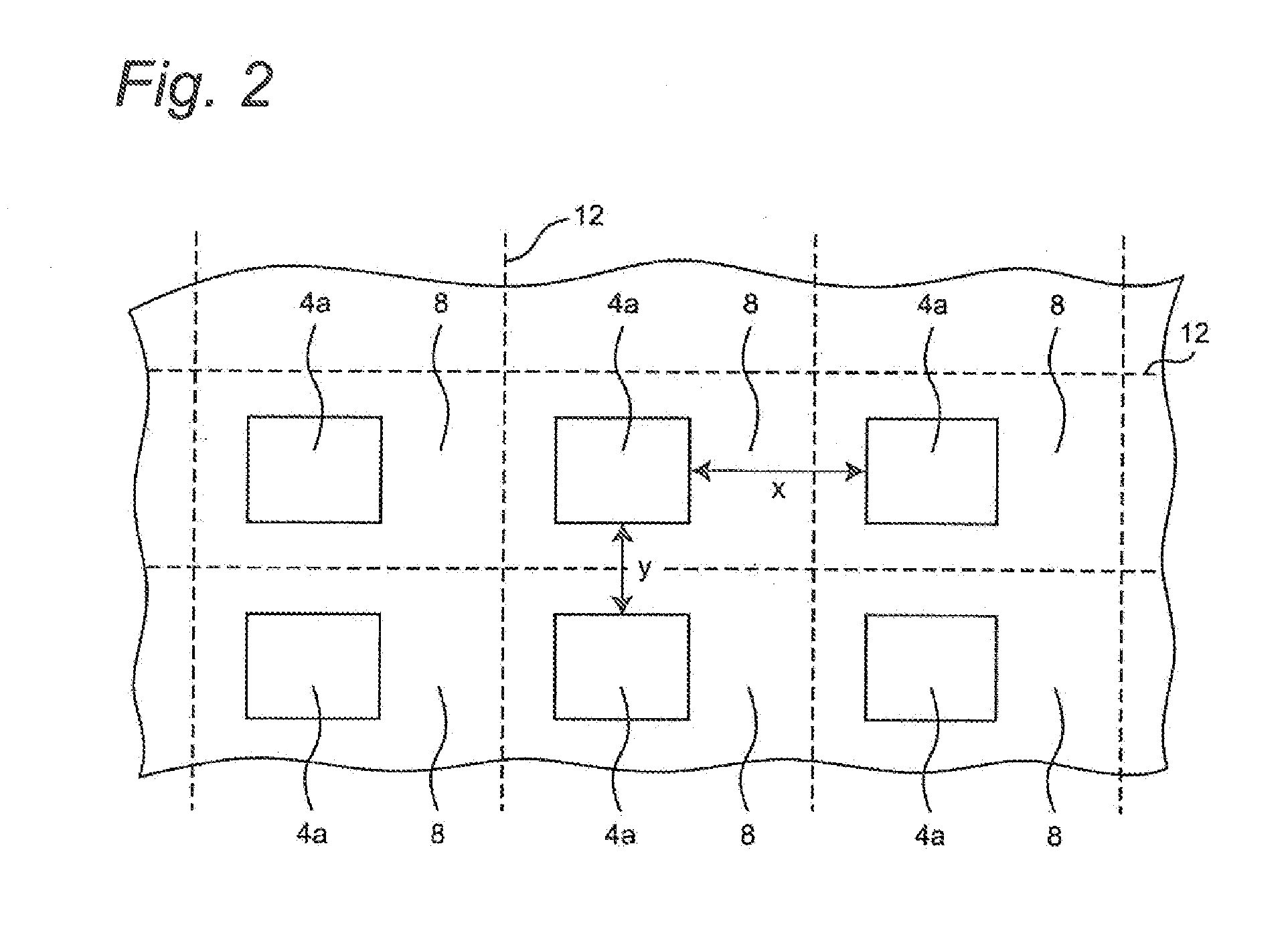
[0036]A method for manufacturing a light emitting device according to this embodiment includes the steps of: disposing a plurality of light emitting elements in a matrix over an aggregate substrate, and disposing a semiconductor element other than the light emitting element in between the adjacent light emitting elements in one of column and row directions of the light emitting elements disposed in the matrix; after disposing phosphor layers over the upper surface of the light emitting elements, disposing a reflective resin to cover the semiconductor elements along the side surfaces of the light emitting elements and the side surfaces of the phosphor layers; and simultaneously cutting the reflective resin and the substrate disposed in between the adjacent light emitting elements in one direction of the column and row directions and between the light emitting element and the adjacent semiconductor element in the other direction so as to include at least one light emitting element and...

second embodiment

[0062]The phosphor layer for use is produced by molding a mixture of the phosphor material and binder, such as resin or glass, into a plate shape. In order to adjust the light emission from the light emitting device to a desired chromaticity, it is often necessary to increase the amount of phosphor material contained in the phosphor layer. Methods for increasing the amount of phosphor material include increasing the concentration of phosphor material, and increasing the thickness of the phosphor layer. As the concentration of some phosphor materials selected is increased, the phosphor layers made of the phosphor material might have its strength reduced. When the thickness of the phosphor layer is increased, the thermal conductivity of the phosphor layer is reduced. As a result, heat generated by the phosphor in the light conversion is stored in the phosphor layer, which might promote thermal degradation of the phosphor or binder, thereby reducing the intensity of fluorescence. Howev...

third embodiment

[0090]FIG. 7 is a schematic cross-sectional view showing the structure of a light emitting device C in this embodiment. The light emitting device C has the same structure as that of the light emitting device of the second embodiment except that the adhesive layer of the second embodiment does not exist in the third embodiment, that a phosphor layer 13 contains a thermosetting binder, and that the phosphor layer 13 is fixed directly to the light emitting element 3.

[0091]FIGS. 8A, 8B, and 8C are exemplary diagrams showing one example of steps of a manufacturing method of the light emitting device C in this embodiment. The manufacturing method of this embodiment can manufacture the light emitting device in the same way as that of the second embodiment except that the phosphor layer containing thermosetting binder is fixed directly to the light emitting element 3 without forming the adhesive layer.

[0092]FIG. 8A shows the step of disposing the light emitting elements over the substrate. ...


PUM


Abstract

A manufacturing method of a light emitting device includes a light emitting element disposed over a substrate and a reflective resin disposed along the side surface of the light emitting element. The method includes disposing light emitting elements in a matrix over an aggregate substrate, and disposing a semiconductor element between the adjacent light emitting elements in one direction of column and row directions of the light emitting elements in the matrix. A reflective resin is disposed to cover the semiconductor elements along the side surfaces of the light emitting elements and the side surfaces of the phosphor layers. The reflective resin and the substrate disposed in between the adjacent light emitting elements is cut in the column or row direction and between the light emitting element and the adjacent semiconductor element in the other direction, to include a light emitting element or a semiconductor element.

Description

BACKGROUND OF THE INVENTION[0001]1. Field of the Invention[0002]The present invention relates to a method for manufacturing a light emitting device that can be used for a display device, an illumination tool, a display, a backlight source of a liquid crystal display, and the like, and a light emitting device manufactured using the same.[0003]2. Description of Related Art[0004]Light emitting diodes (LED) having received attention as a next-generation light source have excellent effect of energy saving as compared to an existing light source, and will be able to be semipermanently used. Applications of the light emitting diode, for example, including a backlight, a vehicle, a lighting board, a traffic light, and a general illuminating light, have been spread industry-wide.[0005]One of the well-known light emitting devices using the LED includes a light emitting element mounted on a mounting substrate with wirings. In recent years, the so-called chip scale package (CSP), that is, a pac...

Claims


Application Information

Patent Timeline
Patent Type & Authority Applications(United States)
IPC IPC(8): H01L33/60
CPCH01L33/60H01L25/0753H01L33/505H01L24/97H01L2224/16225H01L2224/73253H01L2924/12041H01L2924/01322H01L2924/12035H01L33/56H01L33/54H01L2924/00H01L33/48H01L33/483H01L33/52H01L23/28H01L23/31H01L23/3135H01L33/502
Inventor ISHIDA, MASASHISATO, DAISUKEKITAJIMA, TADAYUKI
Owner NICHIA CORP
Why Eureka
Try Eureka