Exposure apparatus and exposure method, and device manufacturing method

a technology of exposure apparatus and manufacturing method, which is applied in the direction of microlithography exposure apparatus, printers, instruments, etc., can solve the problems of reducing the throughput of the apparatus, difficult to cope with such requirements, and difficult to ignore short-term variation of measurement value caused by short-term variation, etc., and achieve the effect of not reducing the throughpu

a technology of exposure apparatus and manufacturing method, which is applied in the direction of microlithography exposure apparatus, printers, instruments, etc., can solve the problems of reducing the throughput of the apparatus, difficult to cope with such requirements, and difficult to ignore short-term variation of measurement value caused by short-term variation, etc., and achieve the effect of not reducing the throughpu

US20140132940A1Active Publication Date: 2014-05-15NIKON CORP

Image

  • Exposure apparatus and exposure method, and device manufacturing method
  • Exposure apparatus and exposure method, and device manufacturing method
  • Exposure apparatus and exposure method, and device manufacturing method

Examples


modified example

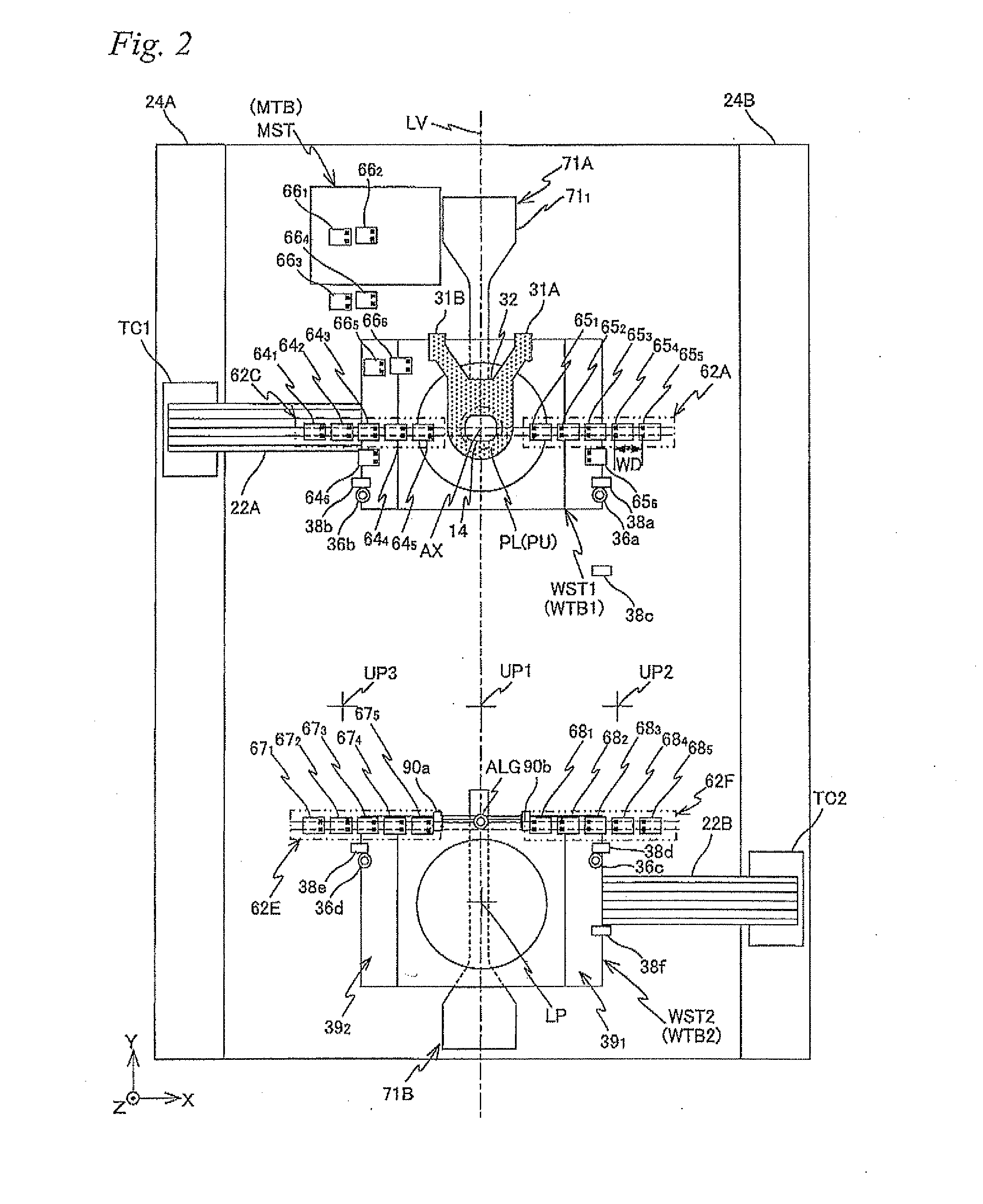
[0264]FIG. 21 shows a state of a moment during concurrent processing operations of the exposure apparatus related to a modified example. FIG. 21 corresponds to a state of FIG. 14 related to the embodiment described previously. As can seen from FIG. 21, in the exposure apparatus related to this modified example, unloading position UP and loading position LP are both set in the vicinity of the measurement arm. To be more specific, when assuming loading position LP of the exposure apparatus related to the embodiment described previously as a reference, loading position LP is set at a position a predetermined distance shifted to the +X side, and unloading position UP is set at a position a predetermined distance shifted to the −X side. And, waiting positions for the wafer such as waiting positions UP2 and UP3 described previously are not provided. Further, in the exposure apparatus related to the modified example, measurement coordinate setting measurement system 35 (imaging sensors 36c...


PUM


Abstract

An exposure apparatus is equipped with a first and second stage that are movable independently from each other within a predetermined plane and each have a table with a grating positioned under a surface where a wafer is mounted, and a third stage that is movable independently from the first and second stages within a predetermined plane and includes a light-receiving plane that receives an energy beam via an optical system. An optical member is provided that is at least a part of a measurement device, which performs a measurement related to exposure based on a light-receiving result of the energy beam received via the light-receiving plane. In an exposure station and measurement station, a first and second measurement system are respectively provided that measure the position of the tables by irradiating the grating of the first or second stage from below with a measurement beam.

Description

BACKGROUND OF THE INVENTION[0001]1. Field of the Invention[0002]The present invention relates to exposure apparatuses, exposure methods and device manufacturing methods, and more particularly to an exposure apparatus and an exposure method used in a lithography process to manufacture electron devices (microdevices), and a device manufacturing method using the exposure apparatus or the exposure method.[0003]2. Description of the Background Art[0004]Conventionally, in a lithography process to manufacture electron devices (microdevices) such as a semiconductor device (an integrated circuit and the like), a liquid crystal display device and the like, a projection exposure apparatus employing a step-and-repeat method (a so-called stepper), or a projection exposure apparatus employing a step-and-scan method (so-called scanning stepper (also called a scanner)) is mainly used.[0005]In this type of exposure apparatus, in general, a position of a wafer stage which moves two-dimensionally whil...

Claims


Application Information

Patent Timeline
15 May 2014
Publication
US20140132940A1
IPC
G03F7/20
CPC
G03F7/70133; G03F7/70733; G03F7/70775; G03F7/70725; G03F7/7085
Inventors
YODA, YASUSHI