Method of producing epitaxial silicon wafer, epitaxial silicon wafer, and method of producing solid-state image sensing device

a solid-state image and silicon wafer technology, applied in the direction of electrical equipment, semiconductor devices, radio frequency controlled devices, etc., can solve the problems of deterioration of semiconductor devices characteristics, increased dark, and formation of defects referred to as white spot defects, so as to suppress metal contamination, reduce the effect of deterioration and improvement of the quality of the semiconductor devi

Active Publication Date: 2014-05-15
SUMCO CORP
View PDF5 Cites 3 Cited by
  • Summary
  • Abstract
  • Description
  • Claims
  • Application Information

AI Technical Summary

Benefits of technology

[0029]According to the method of producing an epitaxial silicon wafer, of the present invention, a silicon wafer including COPs is irradiated with cluster ions thereby forming a modifying layer formed from a constituent elemen

Problems solved by technology

Metal contamination is a major cause of deterioration in characteristics of a semiconductor device.
For example, for a back-illuminated solid-state image sensing device, metal mixed into a semiconductor epitaxial wafer to be a substrate of the device causes increased dark current in the solid-state image sensing device, and results in formation of defects referred to as white spot defects.
In recent years, such metal contaminat

Method used


Image

  • Method of producing epitaxial silicon wafer, epitaxial silicon wafer, and method of producing solid-state image sensing device
  • Method of producing epitaxial silicon wafer, epitaxial silicon wafer, and method of producing solid-state image sensing device
  • Method of producing epitaxial silicon wafer, epitaxial silicon wafer, and method of producing solid-state image sensing device

Examples


examples

[0082]First, single crystal silicon ingots were grown with varied residence time in a temperature range of 1200° C. to 1000° C. (COP formation temperature range). Specifically, single crystal silicon ingots (a) to (d) having four levels of COP formation regions, in which the residence time of the ingots in the COP formation temperature range varies, were grown using three levels of single crystal pulling apparatuses having different hot zone structures at a pulling speed adjusted such that the single crystal silicon ingots to be grown dwell in the temperature range of 1200° C. to 1000° C. for (a) 50 min, (b) 80 min, (c) 150 min, and (d) 160 min.

[0083]Single crystal pulling apparatuses used for growing the above four levels of single crystal silicon ingots (a) to (d) are shown in FIGS. 5A and 5B. A single crystal pulling apparatus 200 shown in FIG. 5A includes, in a chamber 51, a crucible 52 composed of a quartz crucible 52a and a graphite crucible 52b for receiving polycrystalline s...

invention examples 1 to 4

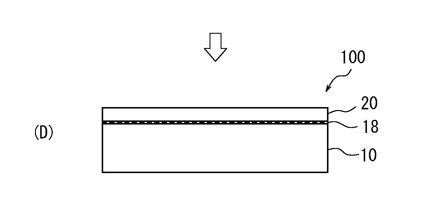
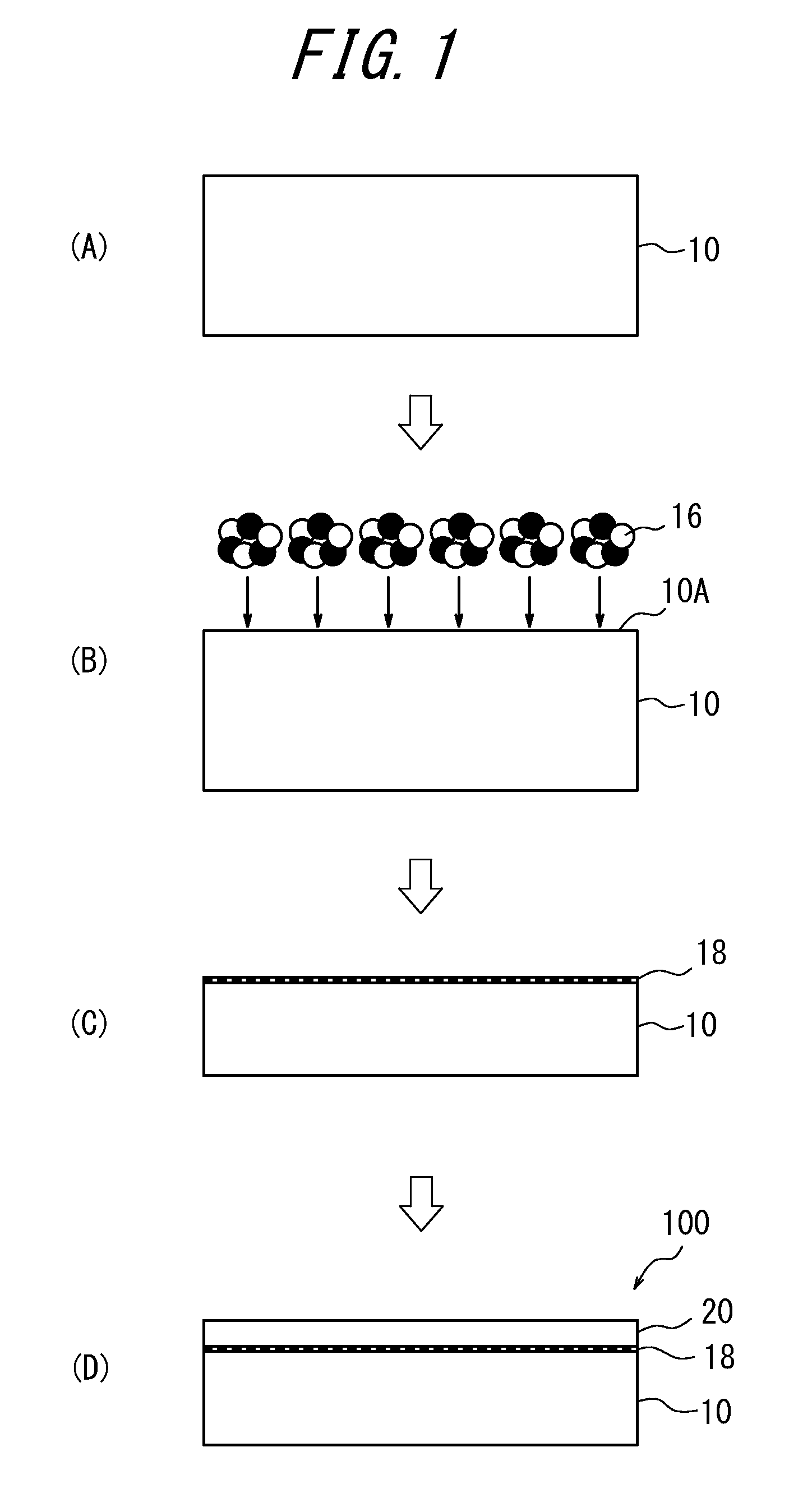
[0093]Subsequently, C5H5 clusters were generated as cluster ions using a cluster ion generator (CLARIS produced by Nissin Ion Equipment Co., Ltd.), and the silicon wafers (a) to (d) fabricated as described above were with the cluster ions under the conditions of dose: 1.00×10¹⁴ Clusters / cm2 (carbon dose: 5.00×10¹⁴ atoms / cm2), and acceleration voltage per one carbon atom: 14.8 keV / atom. After that, each silicon wafers was transferred into a single wafer processing epitaxial growth apparatus (produced by Applied Materials, Inc.) and subjected to hydrogen baking at 1120° C. for 30 s in the apparatus. A silicon epitaxial layer (thickness: 10 μm, kind of dopant: phosphorus, dopant concentration: 1×10¹⁵ atoms / cm3) was then epitaxially grown on the silicon wafer by CVD at 1150° C. using hydrogen as a carrier gas and trichlorosilane as a source gas, thereby obtaining an epitaxial silicon wafer of the present invention. Note that in Invention Examples 1 to 4, irradiation with cluster ions wa...


PUM


Abstract

Provided is an epitaxial silicon wafer with reduced metal contamination achieved by higher gettering capability and a method of efficiently producing the same.
The method of producing an epitaxial wafer includes a wafer production step of pulling a single crystal silicon ingot having a COP formation region by Czochralski process, and subjecting the obtained single crystal silicon ingot to slicing, thereby producing a silicon wafer 10 including COPs; a cluster ion irradiation step of irradiating the produced silicon wafer 10 with cluster ions 16 to form a modifying layer 18 formed from a constituent element of the cluster ions 16, contained as a solid solution in a surface portion 10A of the silicon wafer 10; and an epitaxial layer formation step of forming an epitaxial layer 20 on the modifying layer 18 of the silicon wafer 10.

Description

TECHNICAL FIELD[0001]The present invention relates to a method of producing an epitaxial silicon wafer, an epitaxial silicon wafer, and a method of producing a solid-state image sensing device. The present invention relates in particular to a method of efficiently producing an epitaxial silicon wafer, which can achieve higher gettering capability thereby suppressing metal contamination.BACKGROUND ART[0002]Metal contamination is a major cause of deterioration in characteristics of a semiconductor device. For example, for a back-illuminated solid-state image sensing device, metal mixed into a semiconductor epitaxial wafer to be a substrate of the device causes increased dark current in the solid-state image sensing device, and results in formation of defects referred to as white spot defects. Recently, a back-illuminated image sensing device has been widely used for digital cameras and mobile phones such as smartphones because it can directly receive light from the outside, and take s...

Claims


Application Information

Patent Timeline
IPC IPC(8): H01L21/02H01L27/146H01L29/36
CPCH01L21/02658H01L21/02532H01L29/36H01L27/14687H01L21/02631H01L21/02381H01L21/02576H01L21/0262H01L29/167
Inventor KADONO, TAKESHI
Owner SUMCO CORP
Why Eureka
Try Eureka