Fouling layer detection on an environmental sensor

a detection field and environmental sensor technology, applied in the field of environmental sensors, can solve the problems of inability to correct the reading of the parameters of interest, suffer fouling layer accumulation, etc., and achieve the effect of low cost manufacturing and simplified sensor packaging

Active Publication Date: 2014-06-05
NXP BV
View PDF2 Cites 8 Cited by
  • Summary
  • Abstract
  • Description
  • Claims
  • Application Information

AI Technical Summary

Benefits of technology

[0019]Another way to provide a surface for the environmental sensor is to deposit on the semiconductor substrate a material (for example, an oxide) that can serve as the surface. In this way the packaging of the sensor can be simplified (since no separate provision (such as a window) need be made in the package itself to form the reflecting surface).
[0020]The surface comprising a layer of material deposited on the semiconductor substrate comprises silicon nitride, silicon oxynitride or silicon dioxide. These are materials that are in common use in semiconductor manufacturing further enabling low cost manufacturing.

Problems solved by technology

Environmental sensors will inherently be exposed to the environment and therefore can suffer fouling layer accumulation.
These fouling layers can inhibit correct reading of the parameters of interest.

Method used


Image

  • Fouling layer detection on an environmental sensor
  • Fouling layer detection on an environmental sensor
  • Fouling layer detection on an environmental sensor

Examples


first embodiment

[0040] the light sensor is integrated in a semiconductor substrate. The light sensor can be a simple device such as a light dependent resistor (LDR) or a more advanced device such as one based on photodiodes or phototransistors in the semiconductor substrate that control the flow of holes or electrons across their PN junctions. By combining refraction grids on top of the semiconductor substrate it is possible to let only light at a specific wavelength pass on to the light sensor. The grids can be made during the manufacturing of the different devices in semiconductor substrate from parallel lines made out of polysilicon, dielectric or metal materials. By proper choice of the line spacings, light with different wavelengths can be tuned to reach the light sensor. By combining several light sensors with different grids it is possible to generate an intensity profile at different wavelengths of the received light. This feature can be particularly useful in situations where the nature of...

second embodiment

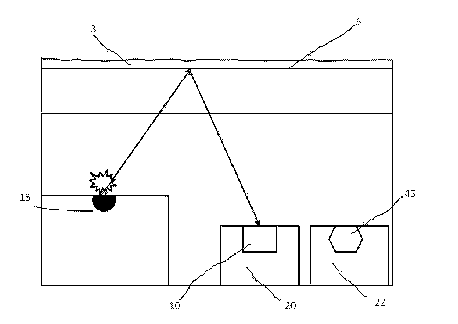
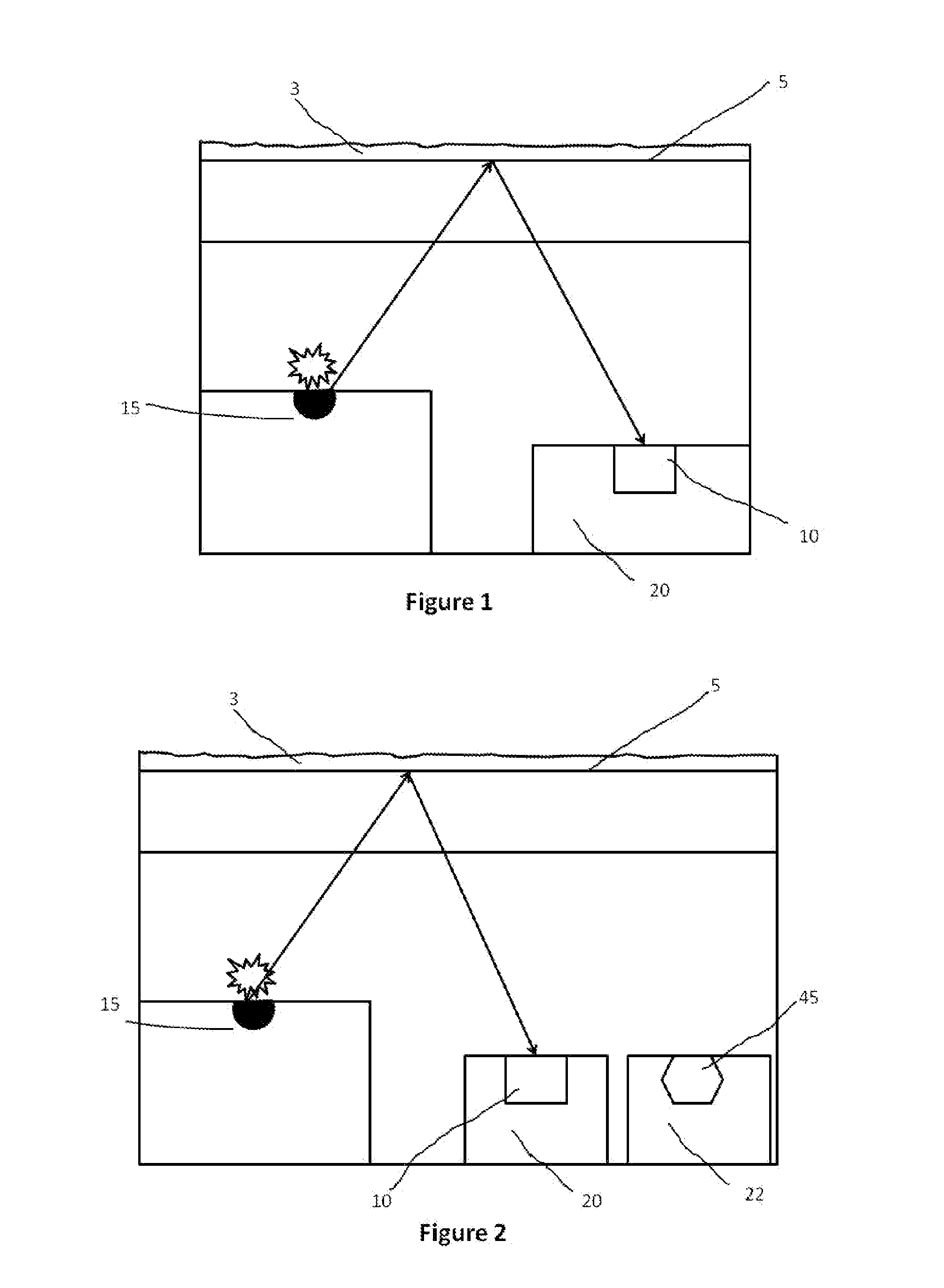
[0041]FIG. 2 schematically illustrates the invention. In accordance with this embodiment, there is provided a light source 15, a light sensor 10 in a semiconductor substrate 20, a surface 5 and a further sensor 45 (for example a temperature sensor) also in a substrate 22. In this way it is possible to extend the environmental sensor with many more sensors that by nature are difficult to integrate in one common semiconductor substrate. For example the light source can be made in a GaN substrate, the light sensor could be made in a CdS substrate and the temperature sensor in a silicon substrate.

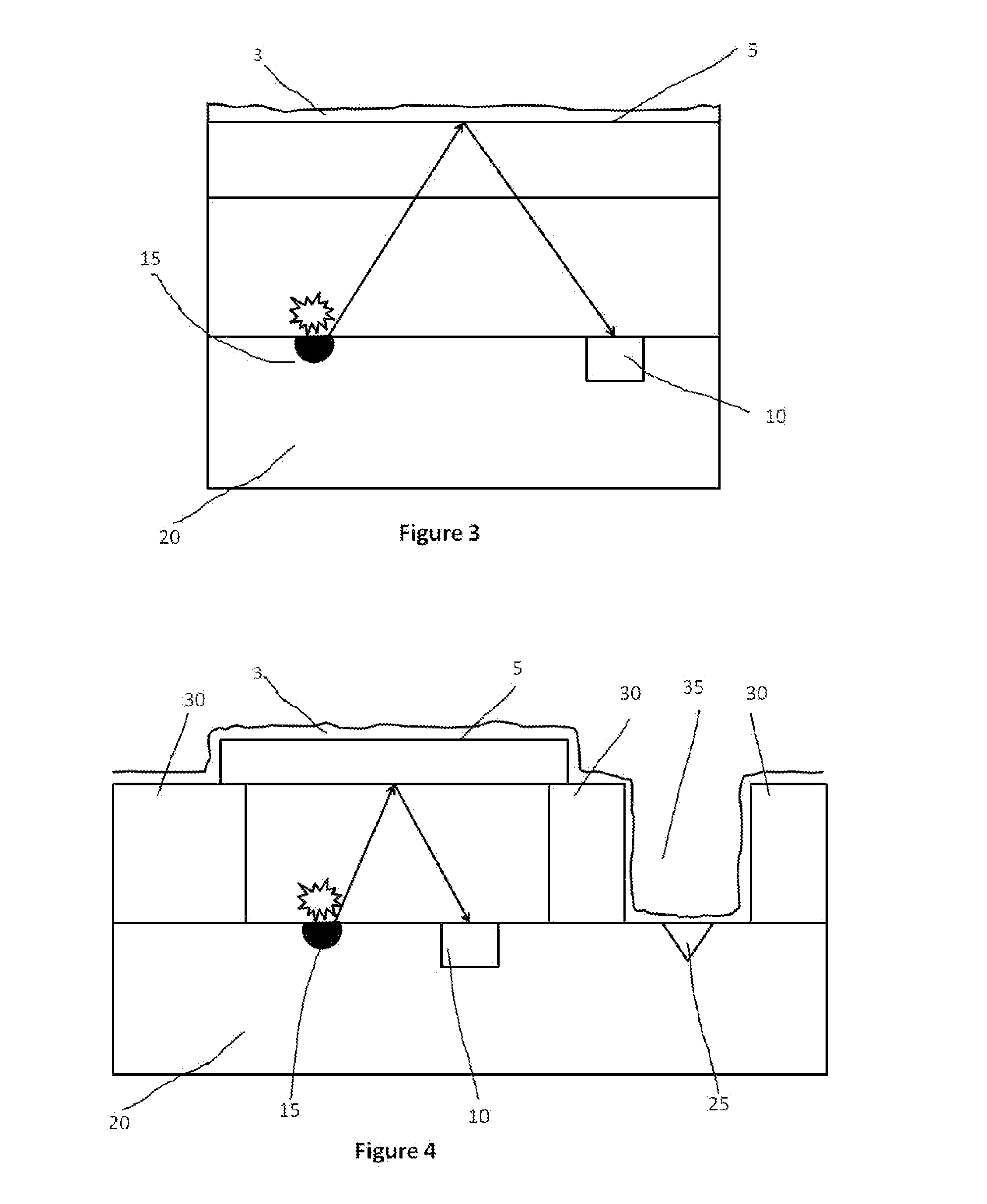
[0042]FIG. 3 schematically illustrates a third embodiment of the invention. In accordance with this embodiment, there is provided a light source 15, a light sensor 10 in a semiconductor substrate 20 and a surface 5. According to this embodiment of the invention, the light source 15 and the light sensor are integrated in a common semiconductor substrate. This embodiment takes advantage of semico...


PUM

PropertyMeasurementUnit
thicknessaaaaaaaaaa
frequency spectrumaaaaaaaaaa
semiconductoraaaaaaaaaa

Abstract

An environmental sensor is disclosed. The environmental sensor includes a semiconductor substrate including a light sensor, a surface through which ambient light can pass to reach a light sensor and a light source operable to illuminate the surface, whereby at least some of the light from the light source is reflected by the surface onto the light sensor. The environmental sensor is operable to determine the presence of a fouling layer on the surface by comparing measurements of ambient light and reflected light by the at least one light sensor.

Description

BACKGROUND OF THE INVENTION[0001]This invention relates an environmental sensor. This invention also relates to a method of operating an environmental sensor.[0002]Environmental sensors can be used for the determination of various physical parameters such as temperature, light intensity, pressure, strain, shock, moisture, carbon dioxide and many other gases in various environments such as buildings (e.g. houses, offices, warehouses, green houses etc.), vehicles such as cars and trucks (for example in the passenger compartment, or in the engine of the vehicle), in-vitro and even in-vivo applications.[0003]There is a clear society trend to make homes and building smart, meaning that the ecological footprint of homes and buildings must be reduced as much possible. A lot of energy in buildings and homes is used in heating, ventilation and air conditioning (HVAC). A carbon dioxide sensor can, for example, monitor the quality of the air and together with a temperature and humidity sensor ...

Claims


Application Information

Patent Timeline
Patent Type & Authority Applications(United States)
IPC IPC(8): G01N21/17
CPCG01N21/15G01N21/53G01N21/94G01N2021/157G01N2021/945G01N21/17
Inventor SYED, ALY AAMERAGARWAL, MANVI
Owner NXP BV
Why Eureka
Try Eureka