X-ray detector

a detector and x-ray technology, applied in the field of x-ray detectors, can solve problems such as current drop, and achieve the effect of reducing the resistance of data lines

Active Publication Date: 2014-06-05
INNOLUX CORP
View PDF3 Cites 13 Cited by
  • Summary
  • Abstract
  • Description
  • Claims
  • Application Information

AI Technical Summary

Benefits of technology

[0020]Moreover, the drain electrode of this aspect can be further electrically connected to the data line through a third conductive via hole. Accordingly, the resistance of the data line can be reduced without the drain electrode being thickened.

Problems solved by technology

Although the thin film transistor can normally work in the condition of the overlapping width being smaller than 1 μm, it may cause current drop.

Method used


Image

  • X-ray detector
  • X-ray detector
  • X-ray detector

Examples


embodiment 1

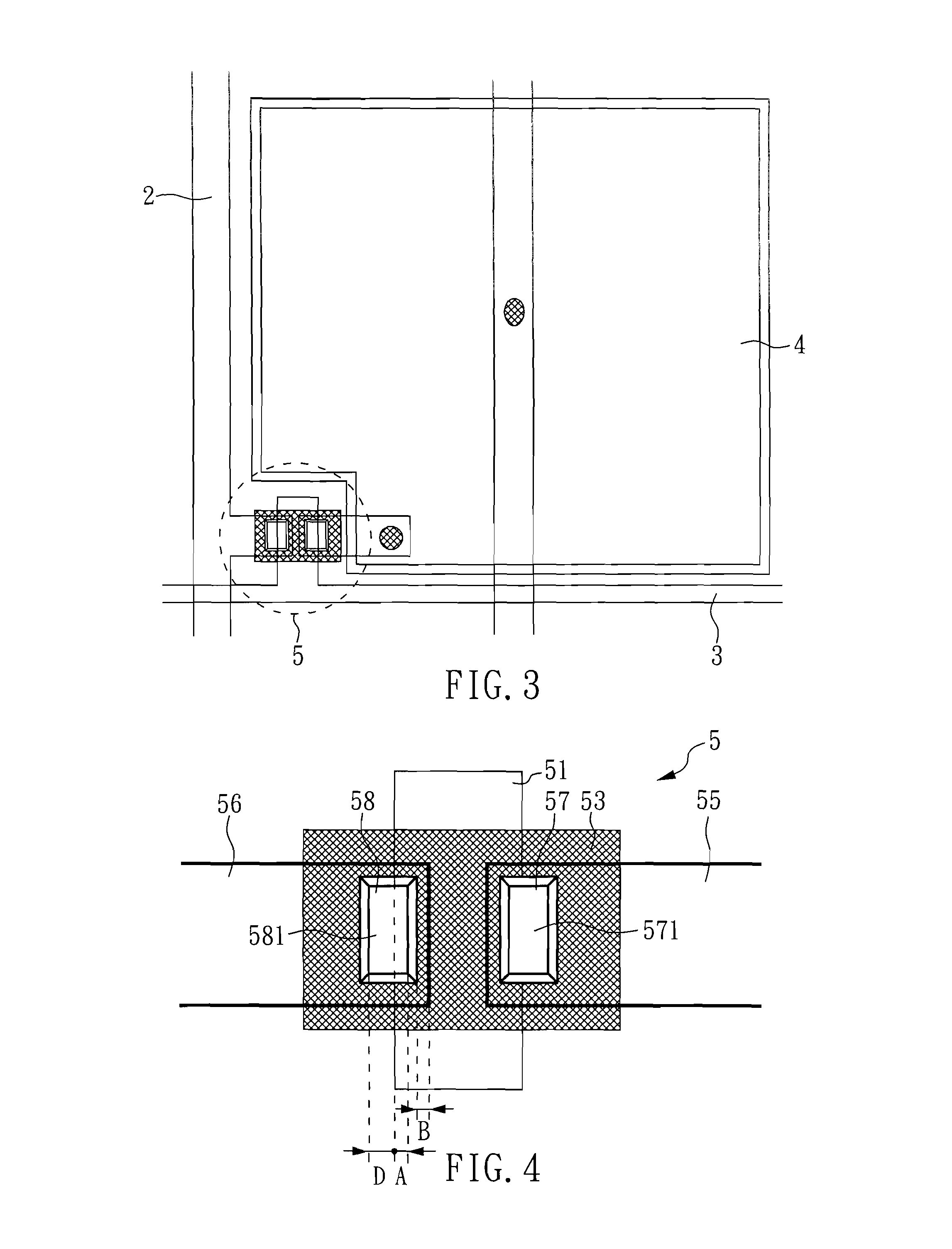
[0034]Referring to FIGS. 3 and 5, FIG. 3 shows a pixel schematic view of an X-ray detector in accordance with Embodiment 1 of the present invention, and FIG. 5 is a cross-sectional view of an X-ray detector including thin film transistors in accordance with Embodiment 1 of the present invention. The X-ray detector of this embodiment includes: a thin film transistor substrate consisting of multiple thin film transistors 5 in an array; a p-i-n photo-diode array layer consisting of multiple p-i-n photo-diodes 6 in an array, in which each p-i-n photo-diode 6 is electrically connected to the corresponding thin film transistor 5; a scintillator layer 7 disposed on the photo-diode array layer; and a reflective layer 8, disposed on the scintillator layer 7. Herein, the thin film transistor substrate includes a substrate 50, a plurality of data lines 2 and a plurality of gate lines 3, and the neighboring data lines 2 and gate lines 3 are intersected to define a plurality of pixel regions 4. ...

embodiment 2

[0038]Referring to FIGS. 6 and 8, FIG. 6 shows a pixel schematic view of an X-ray detector in accordance with Embodiment 2 of the present invention, and FIG. 8 is a cross-sectional view of an X-ray detector including thin film transistors in accordance with Embodiment 2 of the present invention. The X-ray detector of this embodiment is similar to that illustrated in Embodiment 1, except the layout design of the thin film transistor 5.

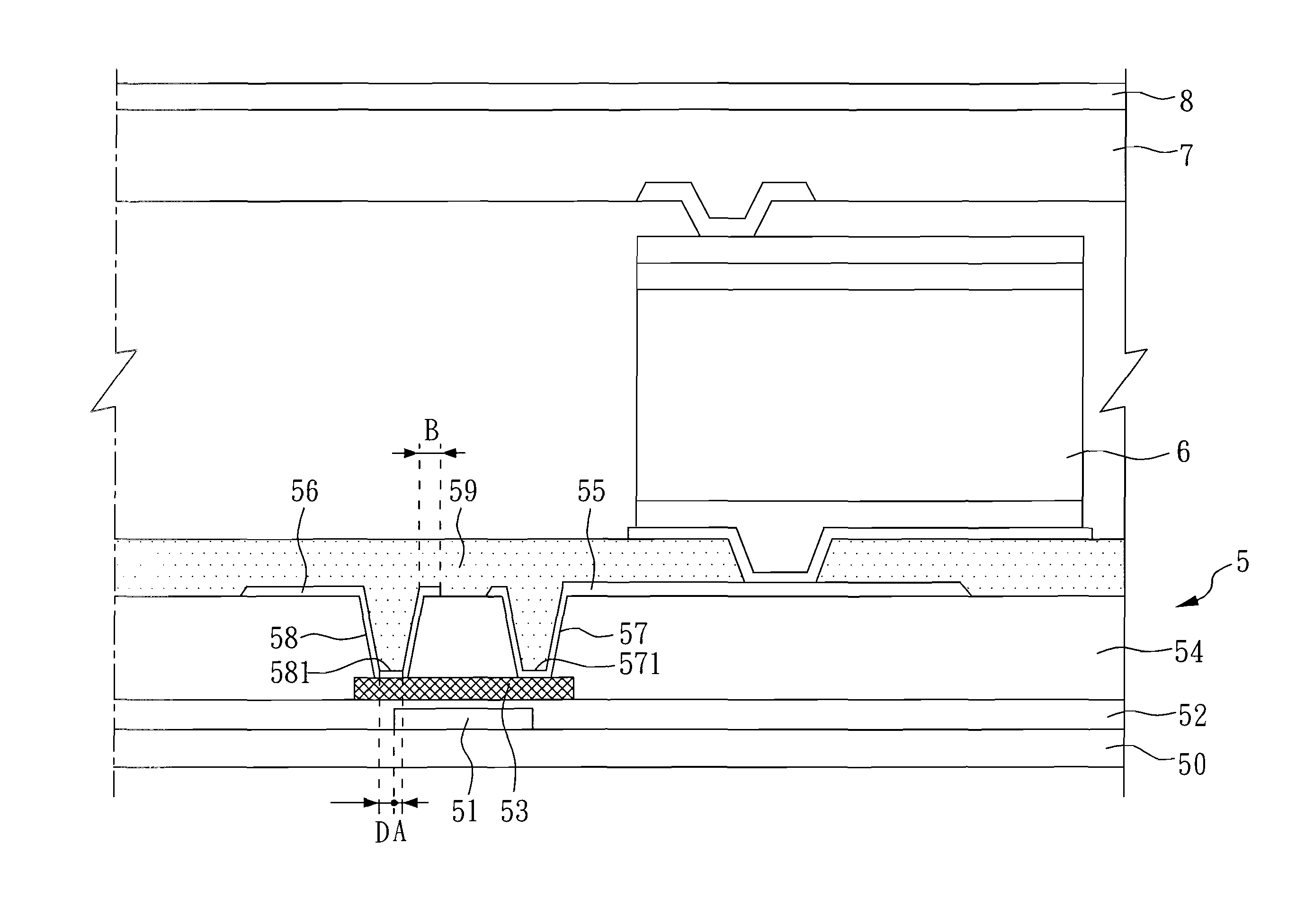
[0039]As shown in FIG. 8 in conjunction with FIG. 7 that shows a top view of the thin film transistor according to Embodiment 2 of the present invention, the thin film transistor 5 forming on the substrate of the thin film transistor substrate of the X-ray detector includes: a gate electrode 51 disposed on the substrate 50; a gate insulating layer 52 disposed on the gate electrode 51; a semiconductor layer 53 disposed on the gate insulating layer 52, wherein the projection area of the semiconductor layer 53 vertically projected on the gate electrode 51 ...

embodiment 3

[0042]FIG. 9 shows a top view of a thin film transistor in accordance with Embodiment 3 of the present invention. This embodiment is similar to Embodiment 2, except that the width of the overlapping region between the projection area of the first and second base portions 571, 581 vertically projected on the substrate 50 and the projection area of the gate electrode 51 vertically projected on the substrate 50 is reduced in this embodiment. This layout design also can reduce the overlapping region between the data line and the gate line, resulting in the decrease of the capacitance value between the data line and the gate line of the thin film transistor.


PUM


Abstract

An X-ray detector including a thin film transistor (TFT) substrate and a photo-diode array layer is disclosed. Each thin film transistor in the TFT substrate includes: a substrate; a gate-electrode on the substrate; a gate insulating layer on the gate-electrode; a semiconductor layer on the gate insulating layer, wherein a portion of the semiconductor layer covers the gate-electrode; an etching stop layer covering the semiconductor layer; a source-electrode and a drain-electrode respectively disposed on the etching stop layer, wherein the source-electrode and the drain-electrode are respectively electrically connected to the semiconductor layer through conductive via-holes each having a base portion at the semiconductor layer, and at least one of the projection areas of the base portions vertically projected on the substrate has a non-overlapping region beyond the projection area of the gate-electrode vertically projected on the substrate; and a passivation layer covering the source-electrode and the drain-electrode.

Description

CROSS REFERENCE TO RELATED APPLICATION[0001]This application claims the benefits of the Taiwan Patent Application Serial Number 101145295, filed on Dec. 3, 2012, the subject matter of which is incorporated herein by reference.BACKGROUND OF THE INVENTION[0002]1. Field of the Invention[0003]The present invention relates to an X-ray detector and, more particularly, to an X-ray detector with improved thin film transistor layout in which the capacitance value between the data line and the gate line can be reduced by decreasing the overlapping area between the data line and the gate line.[0004]2. Description of Related Art[0005]An X-ray detector is a device configured to detect X-ray digital image and can be applied in digital radiography. Compared to screen-film radiography, digital radiography has various advantages, such as better image quality, simple operation process and direct digital image capture.[0006]FIGS. 1 and 2 show top views of conventional InGaZnO thin film transistors (IG...

Claims


Application Information

Patent Timeline
Patent Type & Authority Applications(United States)
IPC IPC(8): H01L29/786
CPCH01L27/124G01T1/241H01L27/14603H01L27/14663H01L27/1225H01L31/085
Inventor WU, CHIH-HAO
Owner INNOLUX CORP
Why Eureka
Try Eureka