Microphone Preamplifier Circuit

Inactive Publication Date: 2014-06-05
OPTIS CIRCUIT TECH LLC
View PDF4 Cites 6 Cited by
  • Summary
  • Abstract
  • Description
  • Claims
  • Application Information

AI Technical Summary

Benefits of technology

The present invention provides a microphone preamplifier circuit that solves problems associated with prior art circuits, such as the inability to reduce PCB area and the consumption of the preamplifier. The circuit includes a preamplifier with a feedback capacitor and a switched capacitor for alternating connection. It also includes an anti-aliasing filter and a DC decoupling capacitor that performs only a DC decoupling function between the microphone circuit's output and the operational amplifier's, without needing a high value. The technical effect is that the circuit reduces the amount of space needed and minimizes power consumption while achieving high pass filtering without the use of a high value DC decoupling capacitor.

Problems solved by technology

However, when it comes to the microphone preamplifying path the implementation of this approach has not been possible due to the huge capacitance value of the decoupling capacitors needed between the microphone and the preamplifier.
In both cases, decoupling capacitors CDEC of more than 100 nF are needed and such large capacitance values would be difficult to integrate in a chip.
In fact, with actual technologies on chip integration of a capacitor having such large capacitance value would require an area greater than 20 mm2 and this fact made the integrating approach practically unusable.
Moreover, unfortunately, even with the PDI methodology the decoupling capacitors CDEC can't be realized because of their high capacitance value and the fact that none of their terminals are connected to a fixed potential.
The same above described problem holds for other consumer devices different from mobile phones, such as portable MP3 players, digital photo cameras, digital audio recorders, video cameras, and in general in devices with audio communication and / or recording and / or processing capabilities.
Moreover, with reference to FIGS. 3 and 4, a further problem of the prior art microphones preamplifiers, especially if they are intended to be embedded in mobile devices, is their power consumption.
However such documents neither refer to microphone systems nor address the above disclosed problem concerning the decoupling capacitor.

Method used


Image

  • Microphone Preamplifier Circuit
  • Microphone Preamplifier Circuit
  • Microphone Preamplifier Circuit

Examples


Embodiment Construction

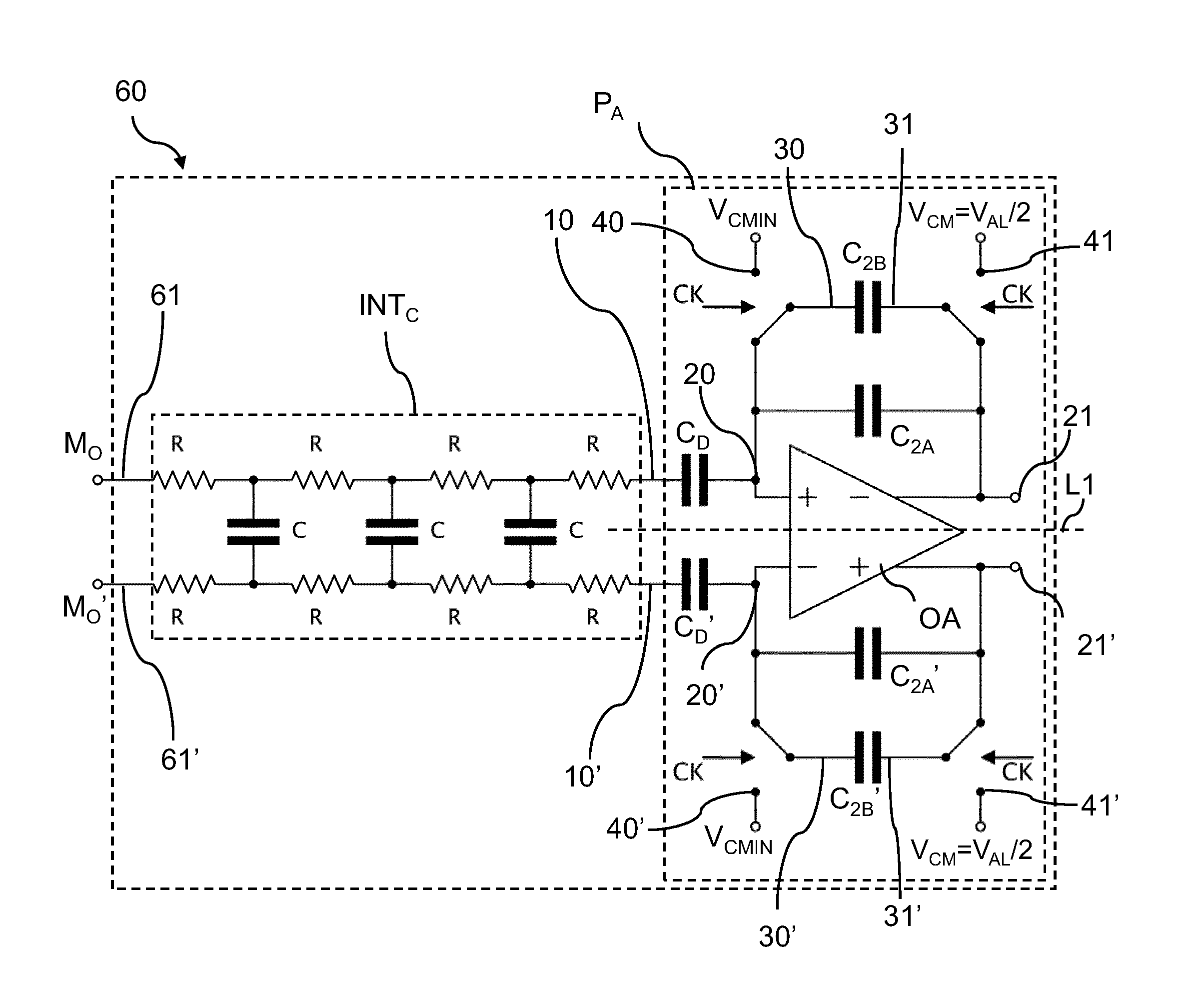
[0030]In the attached figures identical or similar elements will be indicated with the same reference numbers / symbols.

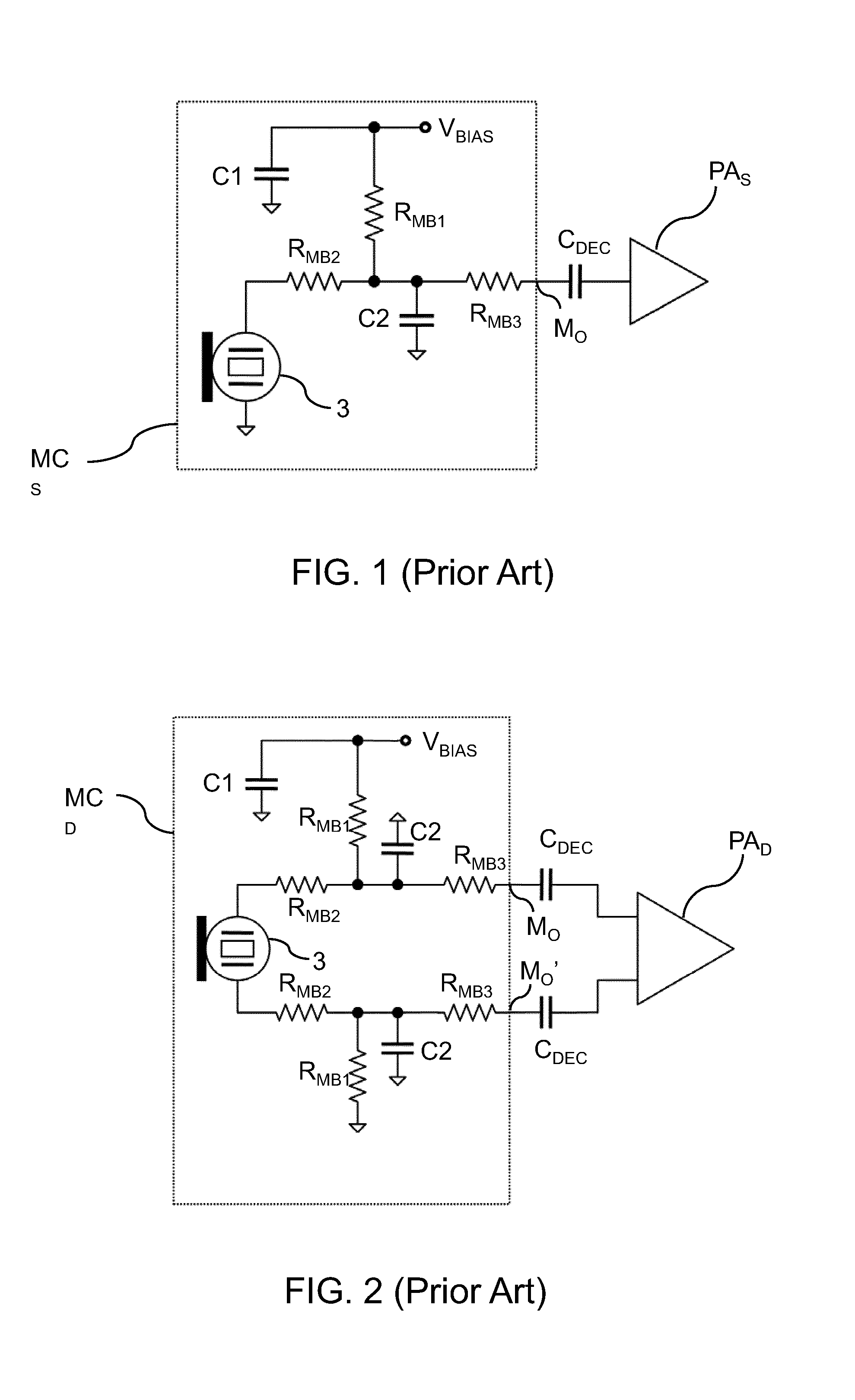
[0031]FIG. 5 shows a very schematic view of an embodiment of mobile terminal 5, such as for example a mobile phone 5, comprising a microphone circuit MCD. According to an embodiment, and without for this reason introducing any limitation, the microphone circuit MCD may be similar to the differential microphone circuit MCD represented in FIG. 2. The microphone circuit MCD comprises a microphone 3, a microphone's biasing network and two differential output nodes MO, MO′ (represented in FIG. 6). According to an embodiment, the microphone's biasing network may be identical or similar to the known biasing network of FIG. 2.

[0032]The mobile phone 5 comprises a circuit board 6 comprising a chip 7 comprising an integrated microphone preamplifier circuit 60. According to the embodiment shown, the circuit board 6 further comprises an analog to digital converter 70 and a digita...


PUM


Abstract

A microphone preamplifier circuit (60) is described, adapted to be connected to a microphone circuit (MCD), the microphone circuit (MCD) comprising a microphone (3) and at least one output node (MO, MO′). The microphone preamplifier circuit (60) comprises a preamplifier (PA) comprising: —at least one input node (10, 10′) adapted to be connected to said output node (MO, MO′); —an operational amplifier (OA) comprising at least one input (20, 20′) and at least one output (21, 21′); —at least one input DC decoupling capacitor (CD, CD′) connected between said input node (10, 10′) and said first input of the operational amplifier (20,20′); at least one feedback capacitor (C2A, C2A′) connected between the input (20,20′) and the output (21, 21′) of the operational amplifier (OA) in order to set together with said input DC decoupling capacitor (CD, CD′) a gain value of the preamplifier circuit (60); —a first (40, 40′) and a second feed node (41, 41′) adapted to be fed by a first (VCIMIN) and a second (VCM) bias voltage respectively. The preamplifier (PA) further comprises at least one switched capacitor (C2B, C2B′) adapted to be selectively and alternatively connected under the control of a clock signal (CK): —between said input (20, 20′) and said output (21, 21′) of the operational amplifier (OA); and—between said first (40, 40′) and said second (41, 41′) feed node.

Description

TECHNICAL FIELD[0001]The present disclosure relates to a microphone preamplifier circuit.BACKGROUND ART[0002]One of the main aspects to take into account in the development of an electronic device, especially mobile devices, is the area occupation. In the field of mobile devices, such as mobile phones, the reduction of the area occupation on the Printed Circuit Board (PCB) is a key point in order to create phones with much more functionalities without altering their dimensions. The focus, during the years, has been to integrate inside a chip, where possible, all those passive components such as resistors, capacitors and inductors which represent the main limit for the area reduction. Inside old generation phones, such passive components were SMD (Surface Mount Devices) mounted directly on the main board. Later on, thanks to improvement in the technology, these devices were placed inside the chip package, a methodology known as PDI (Passive Device Integration), and in some cases dire...

Claims


Application Information

Patent Timeline
IPC IPC(8): H04R3/00
CPCH04R3/00H03F3/005H03F3/187H03F3/45475H03F3/45928H03F3/45937H03F3/45959H03F2203/45512H03F2203/45514H03F2203/45528
Inventor NICOLLINI, GERMANOBARBIERI, ANDREA
Owner OPTIS CIRCUIT TECH LLC
Why Eureka
Try Eureka