Electromagnetic-wave-absorbing film having high thermal dissipation

Inactive Publication Date: 2014-06-05
KAGAWA SEIJI
View PDF4 Cites 23 Cited by
  • Summary
  • Abstract
  • Description
  • Claims
  • Application Information

AI Technical Summary

Benefits of technology

[0009]Accordingly, an object of the present invention is to provide a thin electromagnetic-wave-absorbing film having good absorbability to el

Problems solved by technology

However, because the electromagnetic-wave-absorbing sheet of JP 9-148782 A has regular linear and network patterns, it fails to efficiently absorb electromagnetic waves in a wide frequency range, and suffers large anisotropy in electromagnetic wave absorbability.
However, the electromagnetic wave shield of JP 11-40980 A has insufficient electromagnetic wave absorbability with large anisotropy.
Further, because of linear scratches with irregular widths and irregular intervals, the division of electromagnetic-wave-absorbing films to sma

Method used


Image

  • Electromagnetic-wave-absorbing film having high thermal dissipation
  • Electromagnetic-wave-absorbing film having high thermal dissipation
  • Electromagnetic-wave-absorbing film having high thermal dissipation

Examples


example 1

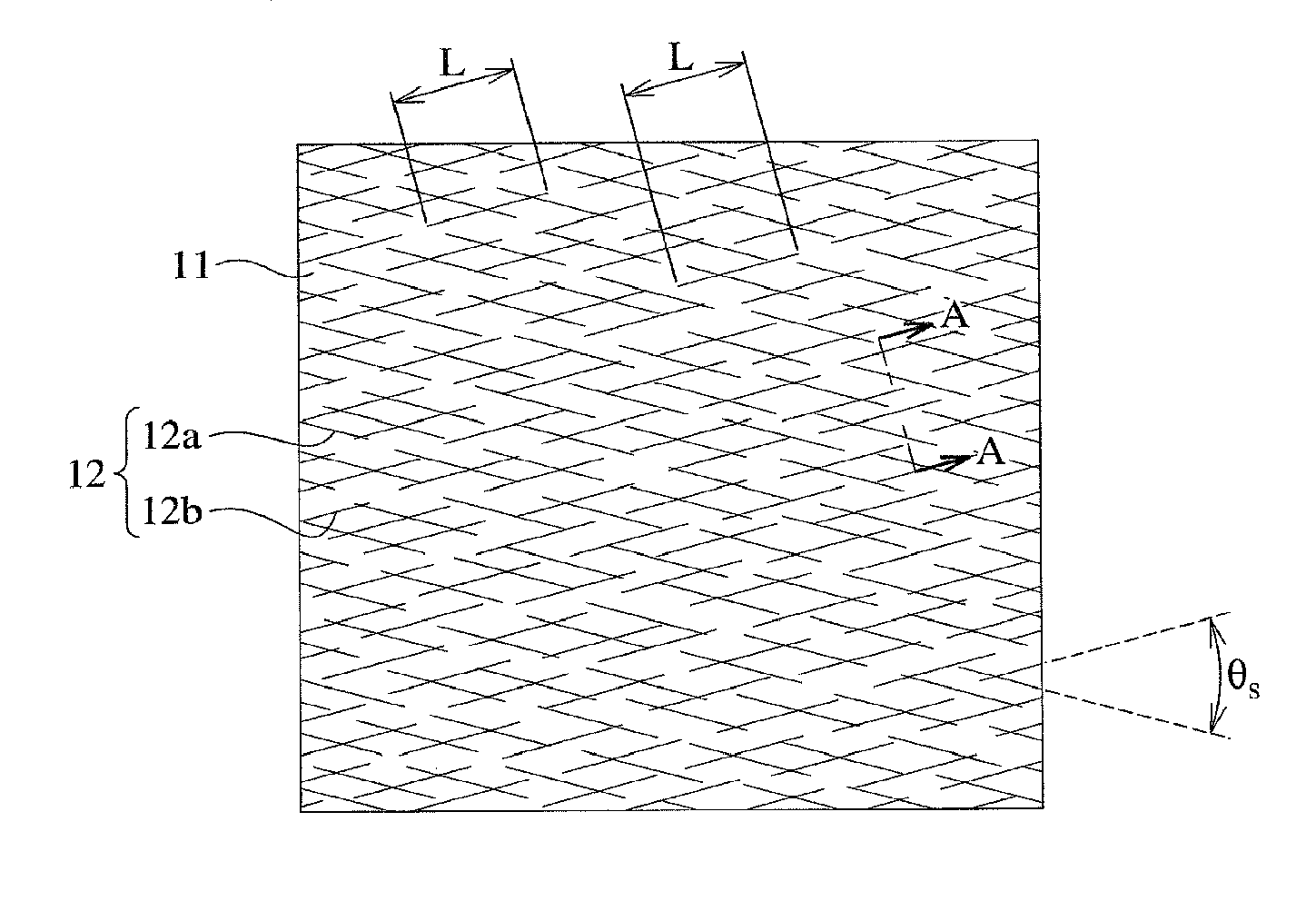
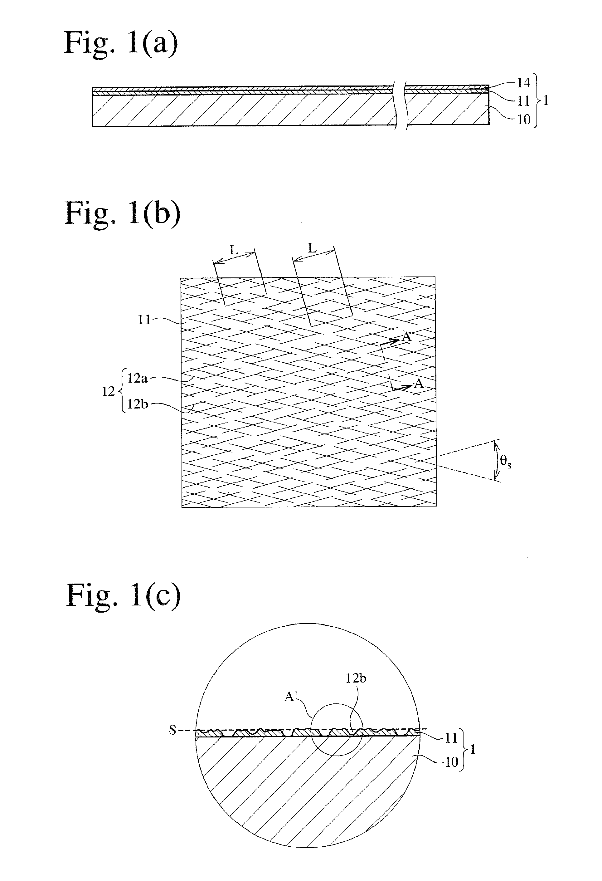
[0133]Using an apparatus having the structure shown in FIG. 9 comprising pattern rolls 32a, 32b having electroplated fine diamond particles having a particle size distribution of 50-80 μm, linear scratches were formed in two perpendicular directions as shown in FIG. 2(c), on a thin aluminum film 11 of 0.05 μm in thickness vacuum-vapor-deposited on one surface of a 16-μm-thick, biaxially oriented polyethylene terephthalate (PET) film. An optical photomicrograph of the linearly scratched, thin aluminum film 11 shows that the linear scratches had the following properties.

Range of widths W0.5-5μm,Average width Wav2μm,Range of intervals I2-30μm,Average interval Iav20μm,Average length Lav5 mm, andAcute crossing angle θs90°.

[0134]A carbon nanotube dispersion comprising 1% by mass of multi-layer carbon nanotube (catalyst removed) having diameters of 10-15 nm and an average length of 3 μm and 1% by mass of a dispersant in methyl ethyl ketone was coated on the linearly scratched, thin aluminu...

example 3

[0140]An electromagnetic-wave-absorbing film 1 was produced in the same manner as in Example 1 except for changing the crossing angle θs of linear scratches to 30°, 60° and 90°, respectively, and the transmission attenuation power ratio Rtp and the noise absorption ratio Ploss / Pin were determined by the same methods as in Example 1 on a test piece TP cut out of each electromagnetic-wave-absorbing film 1. The transmission attenuation power ratios Rtp and the noise absorption ratios Ploss / Pin to the incident wave having a frequency of 6 GHz are shown in Table 1. As is clear from Table 1, high transmission attenuation power ratio Rtp and noise absorption ratio Ploss / Pin were obtained at any crossing angle θs of 30°-90°.

TABLE 1CrossingRtpPloss / PinAngle θs (°)at 6 GHzat 6 GHz3031.00.936032.40.959032.60.96

example 4

[0141]With respect to a test piece TP cut out of each electromagnetic-wave-absorbing film 1 produced in the same manner as in Example 1 except for changing the amount of the carbon nanotube dispersion coated as shown in Table 2 below, the transmission attenuation power ratio Rtp and the noise absorption ratio Ploss / Pin were determined by the same methods as in Example 1. The transmission attenuation power ratios Rtp and the noise absorption ratios Ploss / Pin to the incident wave having a frequency of 6 GHz are shown in Table 2. As is clear from Table 2, when the thin carbon nanotube layer 14 had thickness in a range of 0.01-0.1 g / m2, high transmission attenuation power ratio Rtp and noise absorption ratio Ploss / Pin were obtained, but outside the above thickness range, there were insufficient effects of improving the transmission attenuation power ratio Rtp and the noise absorption ratio Ploss / Pin.

TABLE 2Thickness of ThinRtpPloss / PinLayer of CNT(1) (g / m2)at 6 GHzat 6 GHz—19.90.940.012...


PUM


Abstract

An electromagnetic-wave-absorbing film comprising a plastic film, and a single- or multi-layer thin metal film formed on at least one surface thereof, the thin metal film being provided with large numbers of substantially parallel, intermittent, linear scratches with irregular widths and irregular intervals in plural directions, and coated with a thin carbon nanotube layer.

Description

FIELD OF THE INVENTION[0001]The present invention relates to an electromagnetic-wave-absorbing film having high electromagnetic wave absorbability as well as high thermal dissipation.BACKGROUND OF THE INVENTION[0002]Electromagnetic-wave-absorbing sheets for preventing the leakage and intrusion of electromagnetic waves are used in communications apparatuses such as cell phones, smartphones, wireless LAN, etc., and electronic apparatuses such as computers, etc. Electromagnetic-wave-absorbing sheets now widely used are constituted by metal sheets or nets, and those having metal films vapor-deposited on plastic sheets have recently been proposed. For example, JP 9-148782 A proposes an electromagnetic-wave-absorbing sheet comprising a plastic film, and first and second aluminum films vapor-deposited on both sides thereof, the first vapor-deposited aluminum film being etched to a non-conductive linear pattern, and the second vapor-deposited aluminum film being etched to a conductive netwo...

Claims


Application Information

Patent Timeline
IPC IPC(8): H05K9/00
CPCH05K9/0088H01Q17/002H01L2924/0002Y10T428/24471H01L2924/00
Inventor KAGAWA, SEIJI
Owner KAGAWA SEIJI
Why Eureka
Try Eureka