

Application of Reduced Dark Current Photodetector
a technology of photodetector and dark current, applied in the field of semiconductor-based photodetectors, can solve the problems of limiting device performance, difficult to achieve, and costly cooling of thermoelectric detectors to cryogenic temperatures of around 77 k, and achieve the effect of significantly reducing dark curren
- Summary
- Abstract
- Description
- Claims
- Application Information
AI Technical Summary
Benefits of technology
Problems solved by technology
Method used
Image

Examples
Embodiment Construction
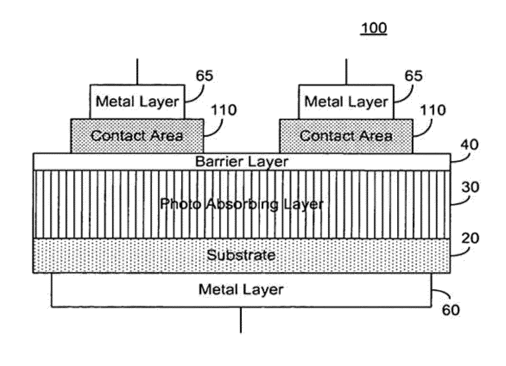
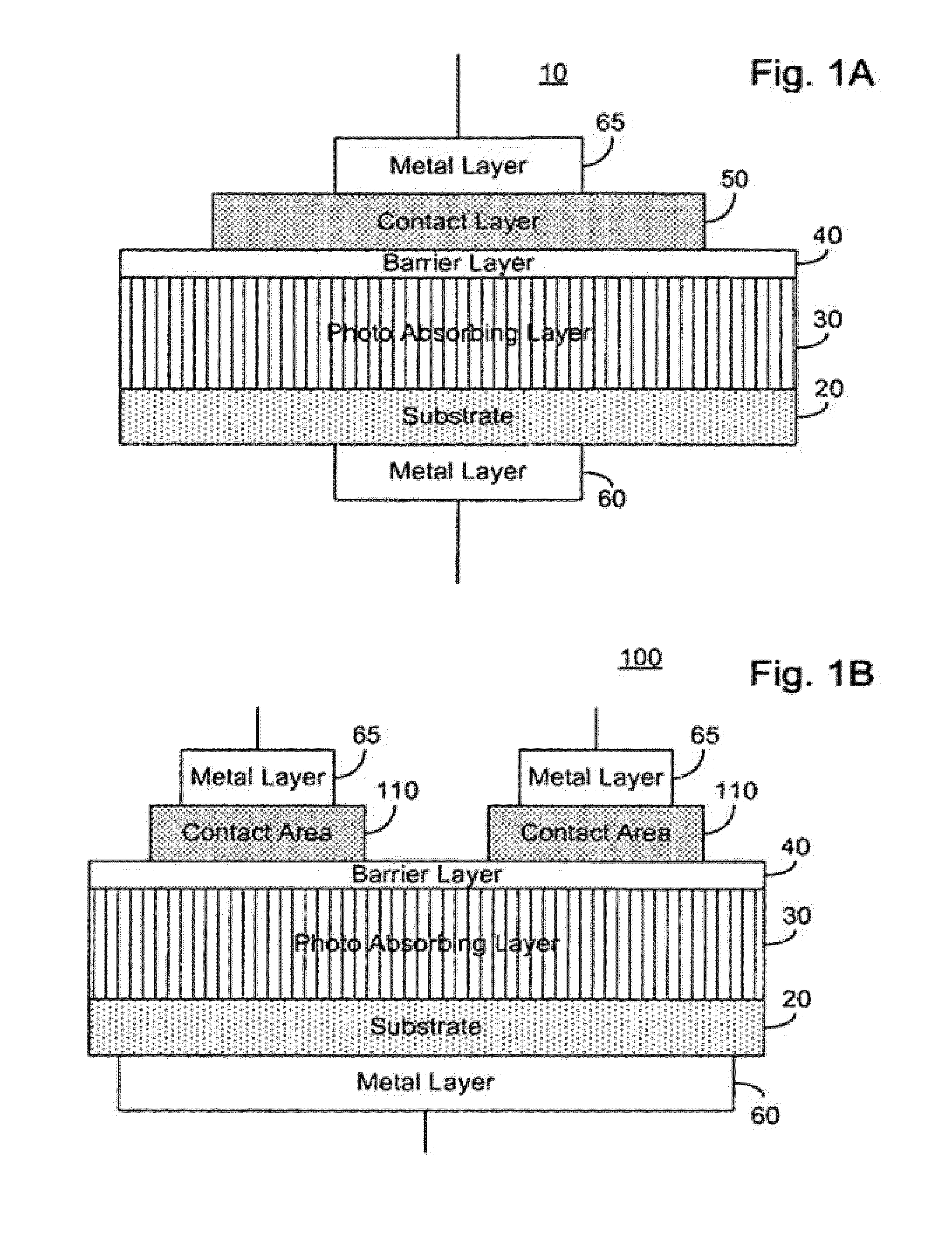
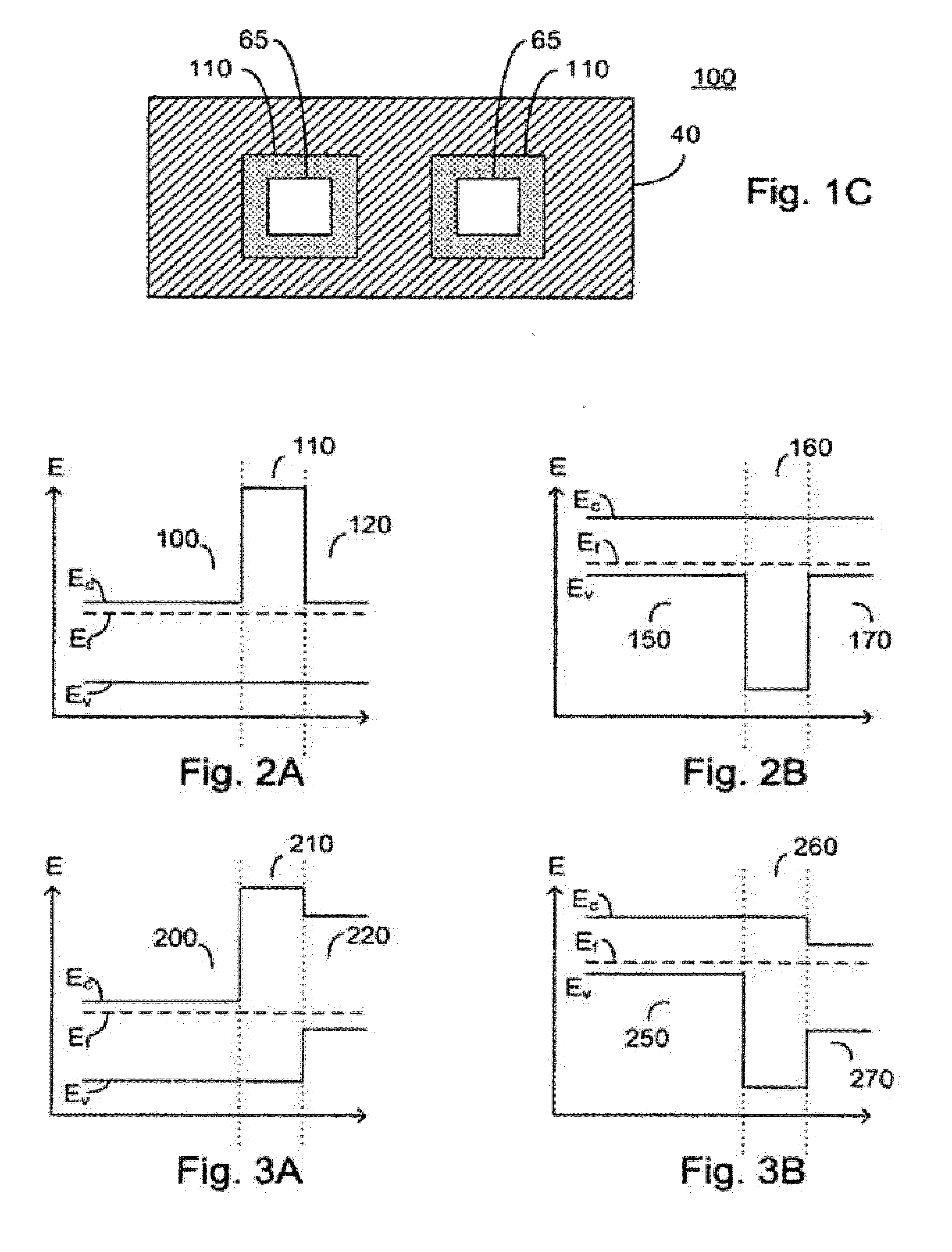
[0050]The present embodiments enable a photo-detector sensitive to a target waveband comprising a photo absorbing layer, preferably exhibiting a thickness on the order of an optical absorption length of the target waveband. In an exemplary embodiment the photo absorbing layer is deposited to a thickness of between one and two times the optical absorption length. A contact layer is further provided, and a barrier layer is interposed between the photo absorbing layer and the contact layer. The barrier layer exhibits a thickness sufficient to prevent tunneling of majority carriers from the photo absorbing layer to the contact layer, and a band gap barrier sufficient to block the flow of thermalized majority carriers from the photo absorbing layer to the contact layer. The barrier layer does not significantly block minority carriers.
[0051]An infra-red detector in accordance with the principle of the invention can be produced using either an n-doped photo absorbing layer or a p-doped pho...
PUM
 Abstract
Description
Claims
Application Information