Semiconductor device

a technology of semiconductors and devices, applied in the direction of logic circuits using specific components, power consumption reduction, pulse techniques, etc., can solve the problem of increasing power consumption due to an increase in leakage current, and achieve the effect of reducing the number of leakage currents

Active Publication Date: 2014-06-12
SEMICON ENERGY LAB CO LTD
View PDF5 Cites 79 Cited by
  • Summary
  • Abstract
  • Description
  • Claims
  • Application Information

AI Technical Summary

Benefits of technology

[0015]It is an object of one embodiment of the present invention to provide a highly reliable semiconductor device. It is an object of one embodiment of the present invention to provide a semiconductor device that is less influenced by a voltage drop. It is an object of one embodiment of the present invention to provide a semiconductor device having low leakage current (off-state current). It is an object of one embodiment of the present invention to provide a novel semiconductor device.
[0018]According to one embodiment of the present invention, it is possible to provide a semiconductor device that can control whether to supply power in each logic element.

Problems solved by technology

With the downsizing of a PLD, an increase in power consumption due to an increase in leakage current becomes a problem.

Method used


Image

  • Semiconductor device
  • Semiconductor device
  • Semiconductor device

Examples


embodiment 1

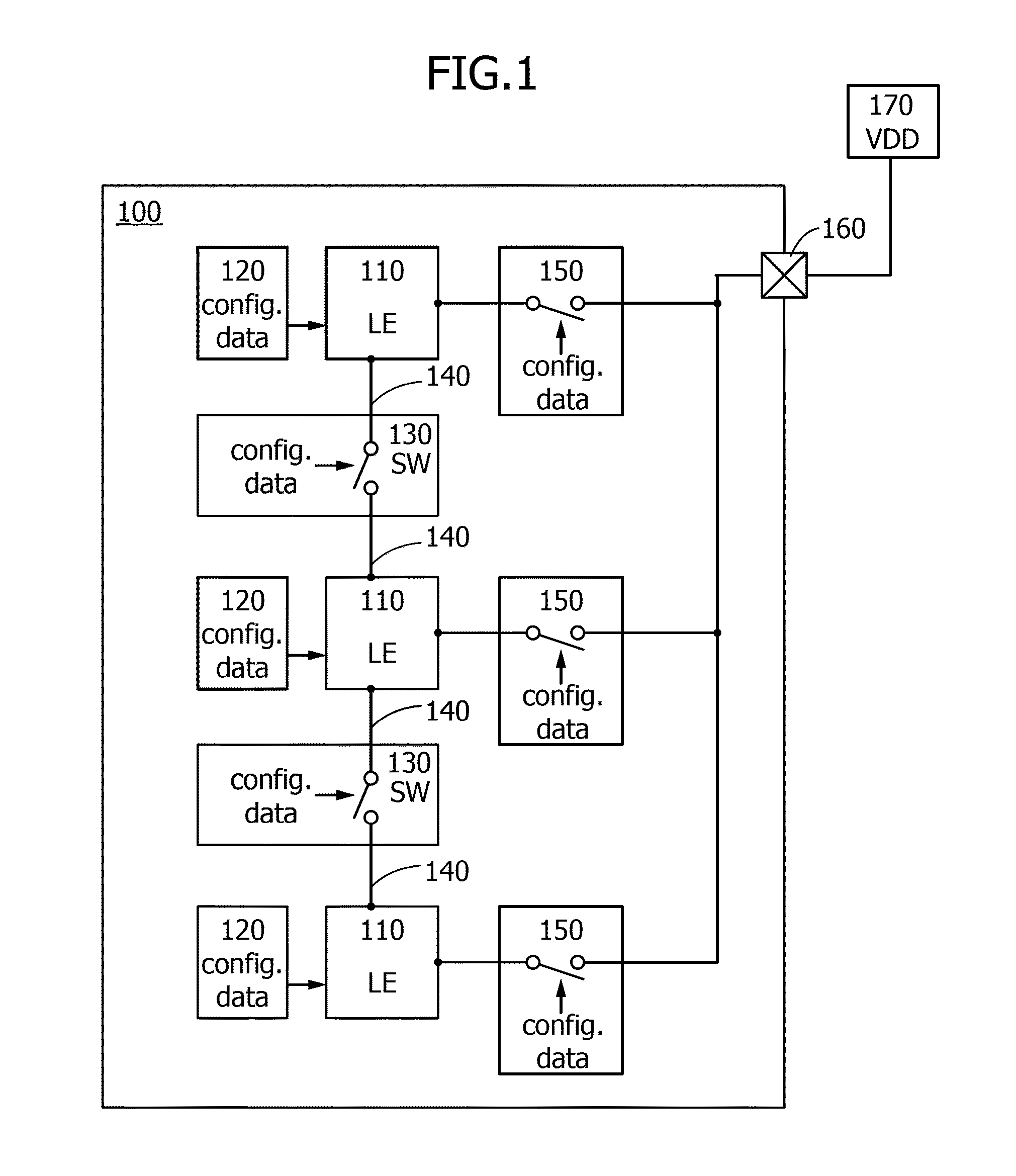
[0048]In this embodiment, a programmable logic device (hereinafter referred to as PLD) is described as an example of a semiconductor device with reference to FIG. 1, FIG. 2, FIG. 3, FIG. 4, FIG. 5, FIG. 6, and FIGS. 7A to 7C.

[0049]Note that examples of user-programmable devices are small-scale integrated circuits such as a programmable array logic (PAL) and a generic array logic (GAL) and large-scale integrated circuits such as a complex programmable logic device (CPLD) and a field programmable gate array (FPGA). In this specification, programmable integrated circuits (including the above integrated circuits) are called PLDs.

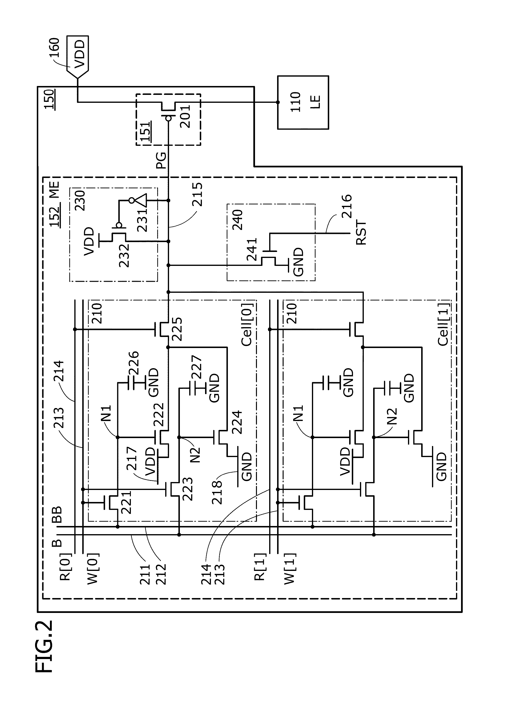
[0050]A PLD in this embodiment includes a circuit (power gating circuit) having a function of switching the operating state (active or non-active) of a logic element with power gating.

[0051]The power gating circuit includes a terminal to which a power supply potential is input from the outside and a programmable switch controlling the conduction state between th...

embodiment 2

[0147]In this embodiment, another structure example of the power gating circuit is described.

[0148]As in Embodiment 1, a power gating circuit in this embodiment has a function of switching the operating state (active or non-active) of a logic element and has a function of changing the value of a potential supplied to the logic element. The power gating circuit includes a switching regulator and a memory storing configuration data.

[0149]The switching regulator has a function of converting the input power supply potential VDD into a potential Vw that is needed for the operation of the logic element by switching a switch and outputting the potential Vw. The memory stores pieces of configuration data for setting the value of the potential Vw output from the switching regulator. The memory can store configuration data corresponding to a plurality of contexts. Specifically, the configuration data is data for setting the conduction state of the switch in the switching regulator.

[0150]The p...

embodiment 3

[0156]In this embodiment, a PLD is described as an example of a semiconductor device.

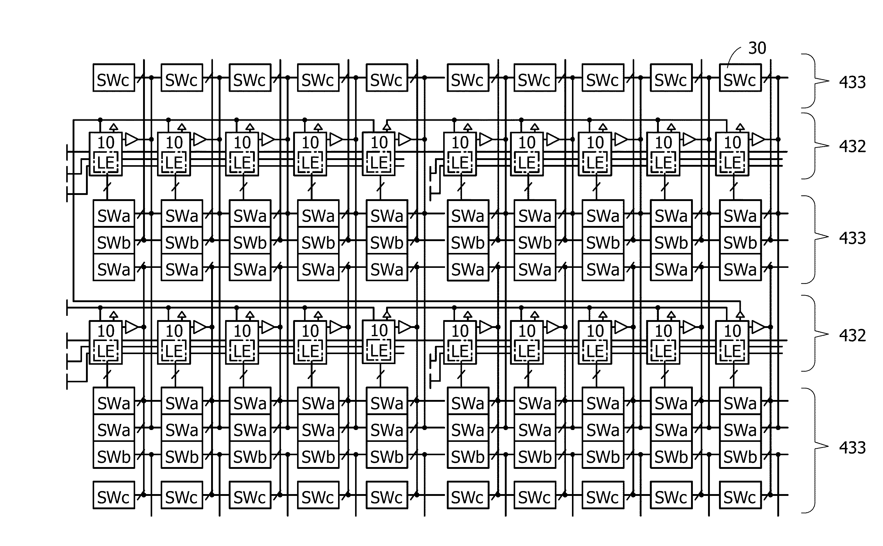
[0157]A PLD in this embodiment also has a function of switching the operating state (active or non-active) of a logic element with power gating. In this embodiment, a PLD in which a switch and a memory element for power gating are provided in a circuit block including a plurality of logic elements is described. This embodiment is described below with reference to FIG. 9, FIG. 10, FIG. 11, FIG. 12, and FIG. 13.

[0158]FIG. 9 is a block diagram illustrating a structure example of a PLD. FIG. 10 is a layout diagram of the structure example. Note that in FIG. 10, some components are denoted by symbols.

[0159]A PLD 400 includes three blocks 401 to 403 including a plurality of internal circuits, a terminal group 404, and a terminal group 405.

[0160]The terminal group 404 includes an input terminal of a power supply potential (e.g., GND or VDD), an input terminal of a signal (e.g., DATA0 or context) from an ex...


PUM


Abstract

A programmable logic device (PLD) that can control whether to supply power in each logic element is provided. The PLD includes at least a programmable logic element, a terminal to which a potential is input from an external power source, a switch controlling conduction between the terminal and the logic element, and a memory outputting a control signal for setting the conduction state of the switch. The memory stores pieces of configuration data for setting the conduction state of the switch. Any one of the pieces of configuration data is output as the control signal from the memory to the switch.

Description

BACKGROUND OF THE INVENTION[0001]1. Field of the Invention[0002]The present invention relates to an object, a method, or a manufacturing method. Further, the present invention relates to a process, a machine, manufacture, or a composition of matter. For example, in this specification, a semiconductor device, a method for driving the semiconductor device, and a method for manufacturing the semiconductor device are described. The present invention relates to a semiconductor device, for example, a circuit having a memory function of storing data, a processor including the circuit having the memory function, or an electronic device including the processor. Further, the present invention relates to a semiconductor device, for example, a display device or a light-emitting device.[0003]Note that in this specification, a semiconductor device means a circuit including a semiconductor element (e.g., a transistor or a diode). The semiconductor device also means any device that can function by ...

Claims


Application Information

Patent Timeline
Patent Type & Authority Applications(United States)
IPC IPC(8): H03K19/00
CPCH03K19/0016H03K19/1776H03K19/17772H03K19/0008
Inventor IKEDA, TAKAYUKIKUROKAWA, YOSHIYUKI
Owner SEMICON ENERGY LAB CO LTD
Why Eureka
Try Eureka