Component-mounting printed board and method of manufacturing the same

Inactive Publication Date: 2014-06-19
FUJIKURA LTD
View PDF0 Cites 6 Cited by
  • Summary
  • Abstract
  • Description
  • Claims
  • Application Information

AI Technical Summary

Benefits of technology

The present invention is a component-mounting printed board and a method of manufacturing it that allows for direct joining of electrodes, reducing thickness and allowing for higher density mounting compared to traditional solder bump connections. The electrode pad of the through-hole electrode is embedded in the resin base, further reducing thickness. The method includes imprinting a circuit pattern, aligning and mounting an electronic component, and then filling the circuit pattern with a conductive paste to form wiring. This direct joining and embedded electrode pad design allows for greater thinning and high density mounting.

Problems solved by technology
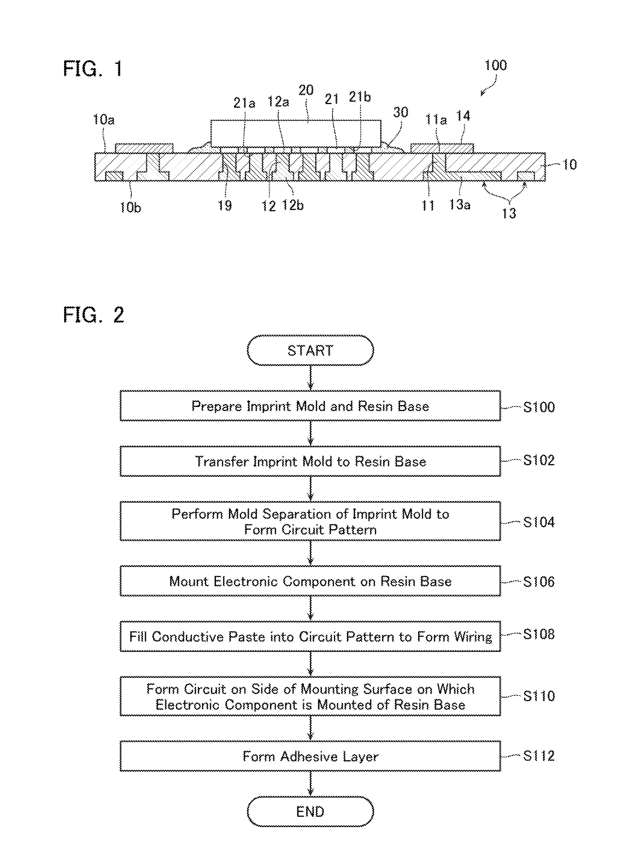
However, in mounting technology such as a BGA system where an electronic component and a wiring board are connected via the likes of a solder bump as in the above-described component-mounting printed board disclosed in Document 1, a diameter of the solder bump attains a size of about 100 μm, hence there is a problem that thinning of the wiring board overall is difficult to achieve.
In addition, a formation pitch of the solder bump is also limited due to the size of the solder bump itself, hence there is also a problem that narrowing of pitch of the electrode pad is difficult to achieve, and mounting by high density wiring is difficult.

Method used


Image

  • Component-mounting printed board and method of manufacturing the same
  • Component-mounting printed board and method of manufacturing the same
  • Component-mounting printed board and method of manufacturing the same

Examples


first embodiment

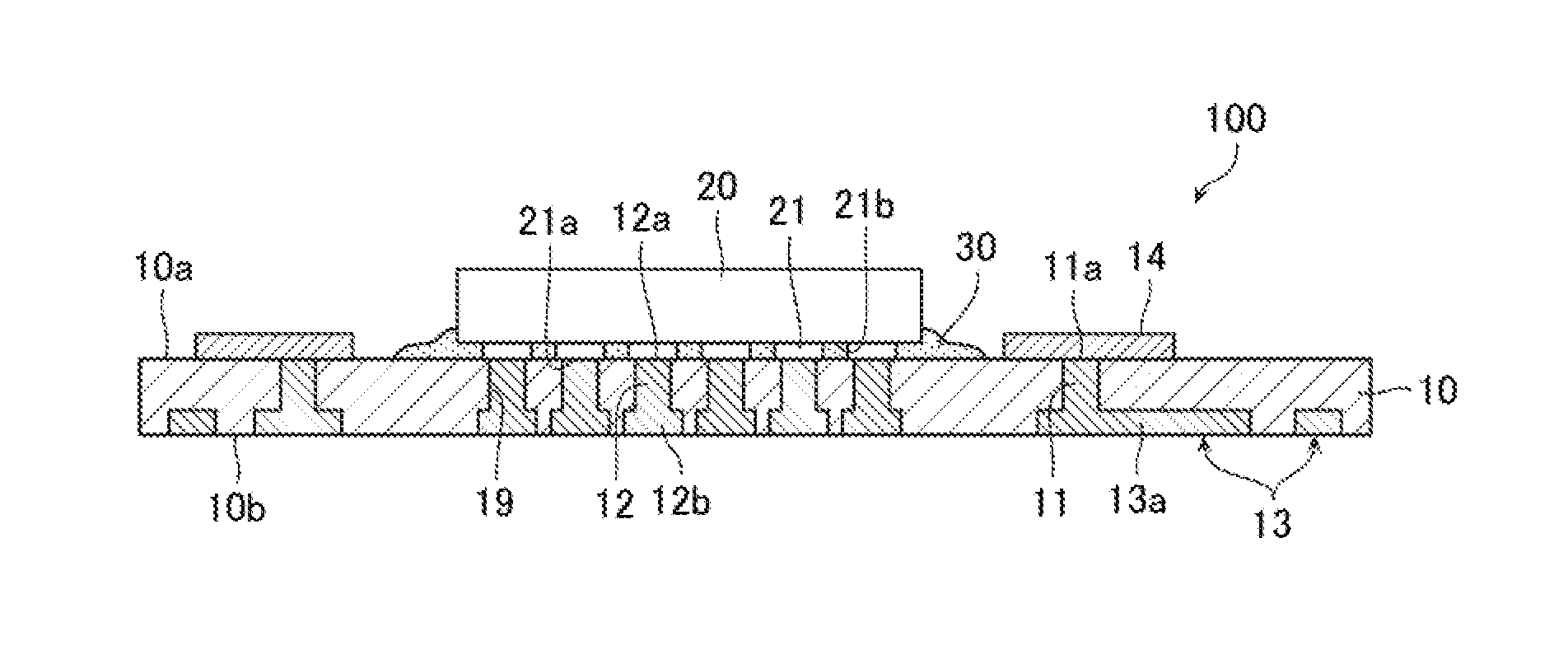
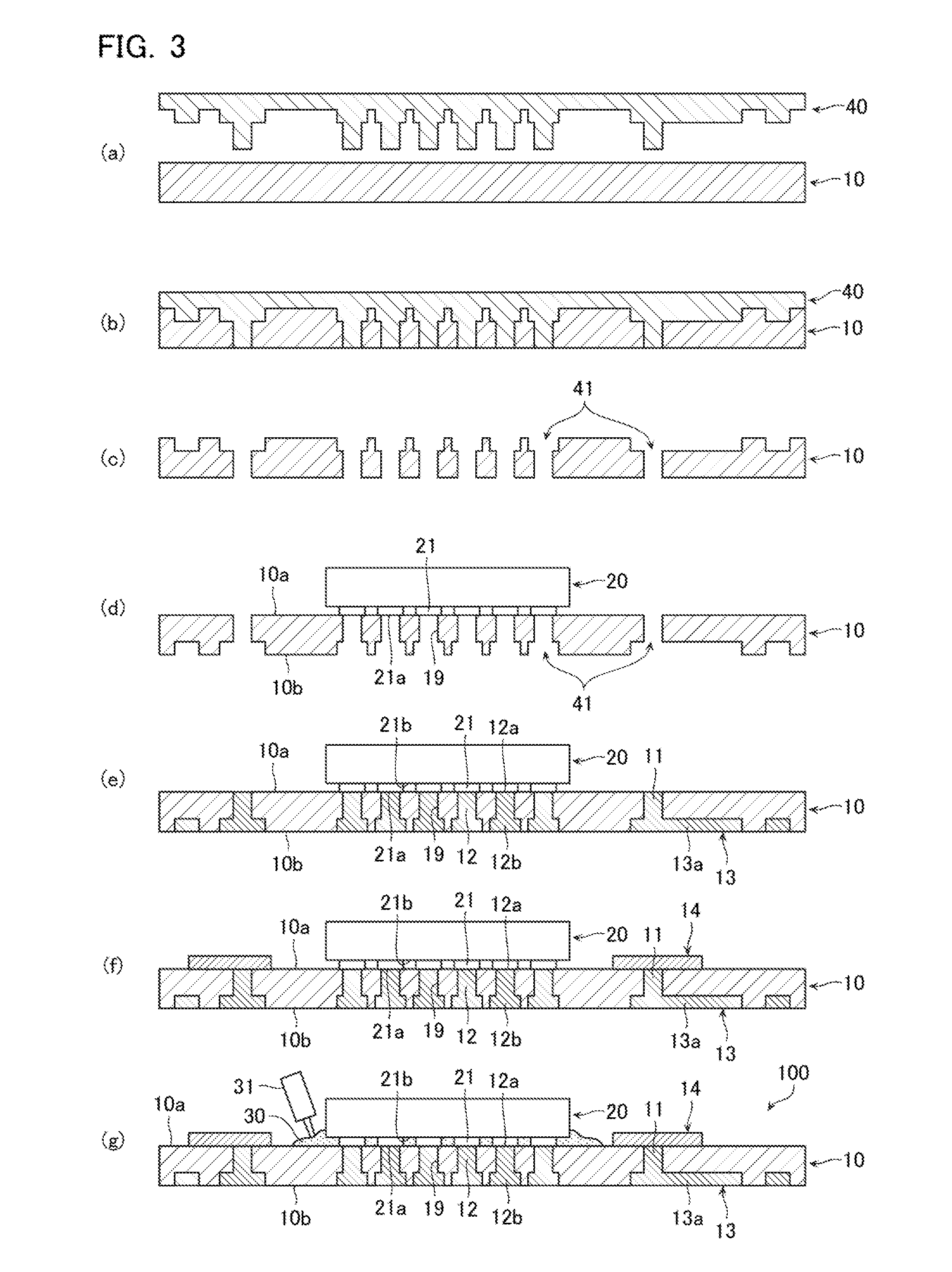
[0035]FIG. 1 is a cross-sectional view showing a structure of a component-mounting printed board according to a first embodiment of the present invention. A component-mounting printed board 100 according to the first embodiment comprises: a resin base 10; and an electronic component 20 mounted on at least one of surfaces, namely a mounting surface 10a, of this resin base 10. In addition, the component-mounting printed board 100 comprises: a through-hole electrode 12 in a through-hole 19 formed in the resin base 10; rear surface wiring 13; and a surface layer circuit 14.

[0036]The resin base 10 is configured by, for example, a resin film having a thickness of about 25 μm. Employable as the resin film are, for example, a resin film configured from the likes of a thermoplastic polyimide, polyolefin, or liquid crystal polymer, or a resin film configured from a thermosetting epoxy resin, and so on.

[0037]The electronic component 20 is a semiconductor component such as an IC chip, and has f...

second embodiment

[0063]FIG. 7 is a cross-sectional view showing a structure of a component-mounting printed board according to a second embodiment of the present invention. A component-mounting printed board 100C according to the second embodiment has a structure, formation process, and so on, of the adhesive layer 30 that differ from those of the component-mounting printed board 100 according to the first embodiment. That is, the adhesive layer 30 is formed only in an underside region of the electronic component 20, and underfill never protrudes outside of the electronic component 20 as in the adhesive layer 30 of the component-mounting printed board 100 according to the first embodiment.

[0064]As a result, the component-mounting printed board 100C according to the second embodiment has similar working effects to those of the component-mounting printed board 100 according to the first embodiment, and by eliminating a protruding portion of the adhesive layer 30 in the mounting surface 10a of the resi...


PUM

PropertyMeasurementUnit
Electrical conductoraaaaaaaaaa
Adhesivityaaaaaaaaaa

Abstract

A component-mounting printed board comprises: a resin base; an electronic component mounted on at least one of surfaces of the resin base; a through-hole electrode formed penetrating the resin base at a position corresponding to an electrode of the electronic component; the electrode of the electronic component and the through-hole electrode being directly joined, and an electrode pad of the through-hole electrode being formed in a surface on an opposite side to a side of a mounting surface on which the electronic component is mounted of the resin base.

Description

CROSS REFERENCE TO RELATED APPLICATIONS[0001]This application is a continuation application of PCT application No. PCT / JP2012 / 071052, filed on Aug. 21, 2012, which is based on and claims the benefit of priority from prior Japanese Patent Application No. 2011-181271, filed on Aug. 23, 2011, the entire contents of which are incorporated herein by reference.BACKGROUND OF THE INVENTION[0002]1. Field of the Invention[0003]This invention relates to a component-mounting printed board having an electronic component surface-mounted thereon, and a method of manufacturing the component-mounting printed board.[0004]2. Description of the Related Art[0005]Known as a conventional component-mounting printed board having an electronic component mounted on a surface thereof is the component-mounting printed board disclosed in Unexamined Japanese Patent Application Publication No. JP 2011-44512 A (Document 1). In this semiconductor component, a solder bump formed on an electrode of an electronic compo...

Claims


Application Information

Patent Timeline
IPC IPC(8): H05K1/11H05K3/30
CPCH05K3/306H05K1/113H01L21/486H01L21/563H01L23/145H01L23/49827H01L23/49894H01L24/19H01L2224/73204H01L2224/92125H05K3/0014H05K3/1258H05K3/305H05K3/4069H05K2201/0129H05K2201/0376H05K2201/10719H05K2201/10977H05K2203/0108H05K2203/1469Y10T29/49133Y02P70/50
Inventor HONDO, TAKAHARU
Owner FUJIKURA LTD
Why Eureka
Try Eureka