Multi-level circuit substrate, method for manufacturing same and method for adjusting a characteristic impedance therefor

Inactive Publication Date: 2005-03-22
PANASONIC CORP
View PDF11 Cites 12 Cited by
  • Summary
  • Abstract
  • Description
  • Claims
  • Application Information

AI Technical Summary

Benefits of technology

It is therefore an object of the present invention to provide, with high density and at low cost, signal-line connection members that are reduced in signal reflection due to a difference i

Problems solved by technology

For data transfer utilizing a high clock frequency, however, the adoption of such a structure cannot provide for sufficient effects to reduce cross talk and control characteristic impedance.
Howeve

Method used


Image

  • Multi-level circuit substrate, method for manufacturing same and method for adjusting a characteristic impedance therefor
  • Multi-level circuit substrate, method for manufacturing same and method for adjusting a characteristic impedance therefor
  • Multi-level circuit substrate, method for manufacturing same and method for adjusting a characteristic impedance therefor

Examples


Example

Now preferred embodiments of the present invention will be described with reference to the drawings.

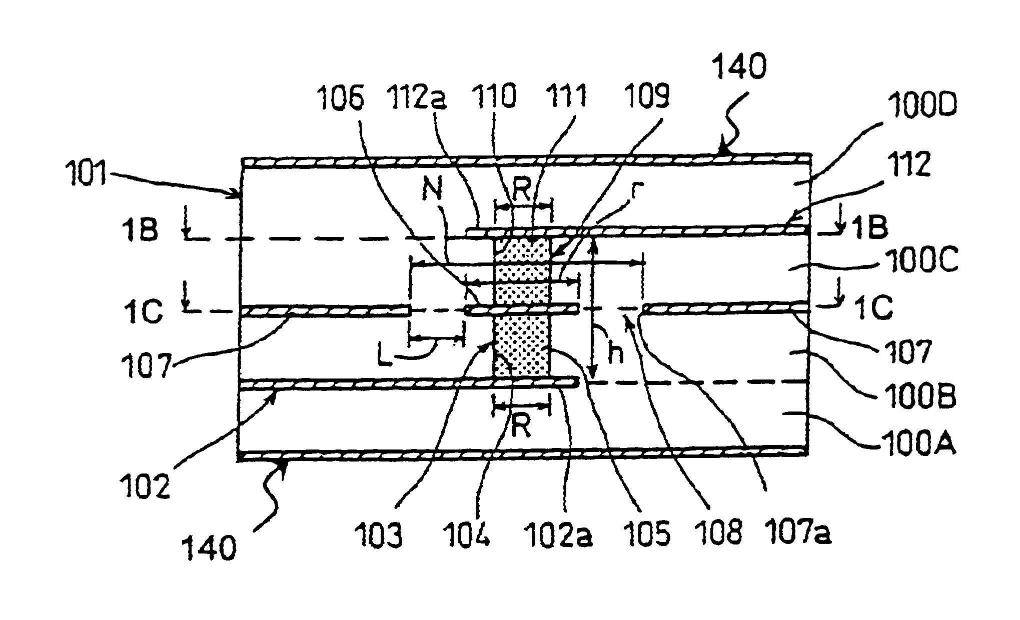
FIG. 1 depicts a structure of a first preferred embodiment of the invention. This embodiment of the invention exemplifies a multi-level circuit substrate having four layers. It is however needless to say that the invention is also applicable to other number of layers than four layers of multi-level circuit substrates.

This multi-level circuit substrate includes a layered body 101 as an example of an insulator. The layered body 101 is structured by integrating four levels of insulation layers 100A, 100B, 100C and 100D. The insulation layer 100A as a lowermost layer of the layered body 101 has, on its top surface, an interconnect layer 102 as an example of a lower-level interconnect layer. The interconnect layer 102 is formed by a conductor film patterned in an interconnection form.

The insulation layer 100A has, at its top surface, an insulation layer 100B as an example of a lower-level ...


PUM


Abstract

An insulator is provided between interconnect layers oppositely placed. The interconnect layers are connected between by connection members provided through the insulator. The connection members at one and the other ends are connected between in their center positions. A shield layer is provided spaced from the intermediate connection layer generally on a same plane as the intermediate connection layer. A condition of (R·r)/(2·h)≦L≦(5·R·r)/h is satisfied, provided that a connection distance between the interconnect layers through the connection members and the intermediate connection layer is h, the connection members where considered generally as a circular cylinder have a diameter R, the intermediate connection layer where considered generally as circular has a diameter r, and a spaced distance between the intermediate connection layer and the shield layer is L. Thus, characteristic impedance is stabilized.

Description

BACKGROUND OF THE INVENTION1. Field of the InventionThe present invention relates to a multi-level circuit substrate having interlayer connection through a conductor filled between layers thereof, a method for manufacturing same and a method for adjusting a characteristic impedance therefor.2. Description of the Related ArtRecently there has been an increasing demand for implementing high density mounting of semiconductor devices with increase in the need to enhance operation speed and improve performances for the computers. In the high end field of super-computers, etc., the ceramic substrate utilized in semiconductor device mounting is structured by two interconnect layers sandwiched between ground layers (or power source layers). This have realized reduction of cross talk and control of characteristic impedance together with high density mounting. For data transfer utilizing a high clock frequency, however, the adoption of such a structure cannot provide for sufficient effects to...

Claims


Application Information

Patent Timeline
IPC IPC(8): H01L23/58H01L23/66H05K1/02H05K1/11H05K1/00H05K3/46
CPCH01L23/66H05K1/024H05K1/0251H01L2223/6616H01L2924/0002H01L2924/3011H05K1/0298H05K1/116H05K2201/0715H05K2201/09454H05K2201/096H05K2201/09718H05K2201/09781H05K2201/09881H01L2924/00
Inventor IWAKI, HIDEKITAGUCHI, YUTAKAOGURA, TETSUYOSHI
Owner PANASONIC CORP
Why Eureka
Try Eureka